Geometries for electrooptic modulation with χ2 materials in silicon waveguides

a silicon waveguide and material technology, applied in the field of electrooptic modulation, can solve the problems of tiny residual silicon, significant nonlinearity of amplifiers in high-speed analog systems, and poling in nano-scale waveguides, and achieve the effect of low drive voltag

Inactive Publication Date: 2013-02-19
UNIV OF WASHINGTON CENT FOR COMMERICIALIZATION
View PDF8 Cites 75 Cited by
  • Summary
  • Abstract
  • Description
  • Claims
  • Application Information

AI Technical Summary

Benefits of technology

[0005]In one aspect, the invention relates to a slot waveguide for providing electrooptic modulation at exceptionally low drive voltage. The apparatus includes electrical contacts, a waveguide coupled between the electrical contacts, and a nonlinear optical material positioned in the slot region. The waveguide includes a first arm and a second arm that are each arranged to define a slot region for confining an optical mode. The slot region has a height, t1, and each of the first arm and the second arm include a strip load region having a height that is less than the height, t1, of the slot region. Each of the first arm and the second arm is configured to provide an electrical signal to the slot region via at least one of the electrical contacts.

Problems solved by technology

These additional amplifiers can be a significant source of nonlinearity in high-speed analog systems.
Significant challenges exist (e.g. challenges with poling and charge injection at the surfaces) in integrating these high activity materials into the silicon slot waveguide system.
It has emerged that poling in these nanoscale waveguides is a significantly different problem from that of poling larger all-organic or sol-gel / organic devices.
Fabrication imperfections may cause some of the narrower slots to have tiny amounts of residual silicon or oxide in their centers, or to even be partially fused in places.
However, as long as electrical isolation is obtained, and the optical loss is acceptable, we would expect the slot performance to decrease only in a linear proportion to the amount of the slot volume that is no longer available to the nonlinear polymer cladding.
In general, one of the challenges with slot waveguide based modulators is the need to electrically contact each arm (typically silicon) of the slot waveguide with a low resistance electrical path.
In general, one of the challenges with χ2 polymer based devices is that they must have their nonlinear moments oriented in a single direction in order to allow modulation to occur.
For example, it is contemplated that such devices can be used for the probing of RF transmission lines on printed circuit boards where today's approaches tend to require placing probes directly into the signal path, which tends to change the performance of the device under test.

Method used


Image

  • Geometries for electrooptic modulation with χ<sup>2 </sup>materials in silicon waveguides
  • Geometries for electrooptic modulation with χ<sup>2 </sup>materials in silicon waveguides
  • Geometries for electrooptic modulation with χ<sup>2 </sup>materials in silicon waveguides

Examples


Embodiment Construction

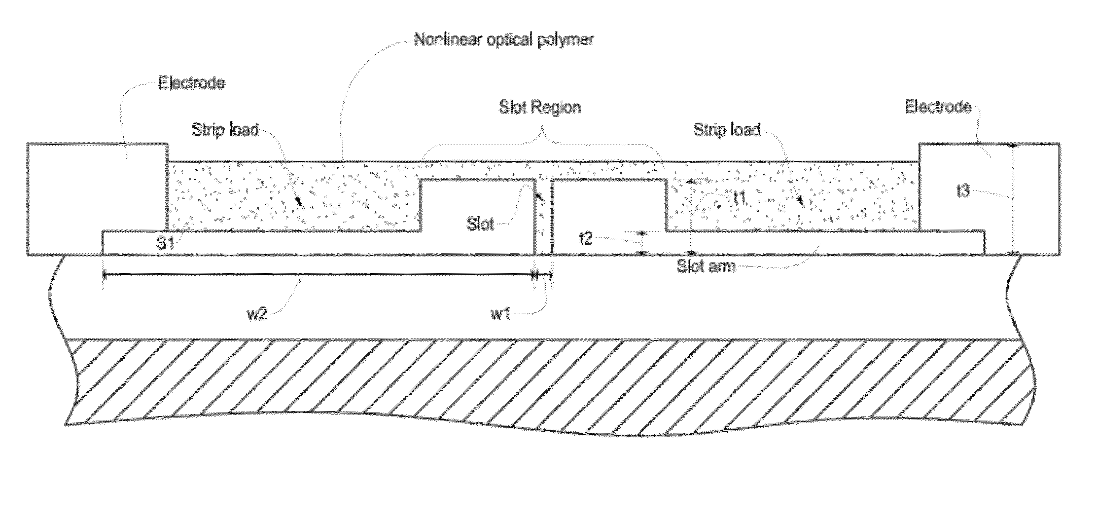
[0053]We describe hereinbelow an apparatus for providing electrooptic modulation. The apparatus may be based on a slot waveguide that is at least partially clad with a nonlinear optical polymer, which can, for example, be fabricated in a silicon-polymer integrated photonics technology. We have previously described such a suitable low drive voltage modulator device in detail in U.S. patent application Ser. No. 12 / 626,561, ALL OPTICAL MODULATION AND SWITCHING WITH PATTERNED OPTICALLY ABSORBING POLYMERS, and in U.S. patent application Ser. No. 12 / 630,833, PHASE MATCHING FOR DIFFERENCE FREQUENCY GENERATION AND NONLINEAR OPTICAL CONVERSION FOR PLANAR WAVEGUIDES VIA VERTICAL COUPLING, both of which applications are incorporated herein by reference in their entirety for all purposes. We begin with a brief technology overview followed by a description of exemplary slot waveguides and Mach Zehnder-based designs suitable for use in the inventive apparatus.

[0054]We now describe high index cont...


PUM

PropertyMeasurementUnit
widthaaaaaaaaaa
height t1aaaaaaaaaa
height t1aaaaaaaaaa

Abstract

An apparatus for providing electrooptic modulation. The apparatus includes electrical contacts, a waveguide coupled between the electrical contacts, and a nonlinear optical material positioned in the slot region. The waveguide includes a first arm and a second arm that are each arranged to define a slot region for confining an optical mode. The slot region has a height, t1, and each of the first arm and the second arm include a strip load region having a height that is less than the height, t1, of the slot region. Each of the first arm and the second arm is configured to provide an electrical signal to the slot region via at least one of the electrical contacts. In one embodiment, the nonlinear optical material includes a χ2-based material. In another embodiment, each of the first arm and the second arm have an “L”-type shape.

Description

CROSS-REFERENCE TO RELATED APPLICATIONS[0001]This application claims priority to and the benefit of co-pending U.S. provisional patent application Geometries for Electrooptic Modulation with χ2 Materials in Silicon Waveguides Ser. No. 61 / 268,173, filed Jun. 9, 2009, which is incorporated herein by reference in its entirety.FIELD OF THE INVENTION[0002]The invention relates to electrooptic modulation in general and particularly to slot waveguides configured for electrooptic modulation.BACKGROUND OF THE INVENTION[0003]A slot waveguide is an optical waveguide that guides light and strongly confines the guided light by capitalizing on the discontinuity of an electric field at high-refractive-index-contrast interfaces. A slot waveguide typically includes two regions of high-refractive-index material separated by a gap, or slot, having a low-refractive-index. The high-refractive-index material is typically covered by a cladding material.[0004]Nonlinear electrooptic polymers can be used as ...

Claims


Application Information

Patent Timeline
Patent Type & Authority Patents(United States)
IPC IPC(8): G02B6/10G02B6/26G02B6/34G02F1/035
CPCG02F1/2257G02F1/355G02F2001/212G02F2001/3505G02F2203/15G02F2201/126G02F2201/127G02F2202/022G02F2202/36G02F2201/06G02F1/025G02F1/212G02F1/3505
Inventor HOCHBERG, MICHAELBAEHR-JONES, THOMAS W.
Owner UNIV OF WASHINGTON CENT FOR COMMERICIALIZATION
Why Eureka
Try Eureka