Plasma CVD apparatus, method for forming thin film and semiconductor device

a technology of plasma cvd and thin film, applied in the direction of plasma technique, solid-state diffusion coating, semiconductor/solid-state device details, etc., can solve the problems of failure to maintain the dielectric constant and mechanical strength, insufficient insulating property, etc., to achieve high mechanical strength, stably maintained, and high mechanical strength

Inactive Publication Date: 2013-03-26
MITSUBISHI ELECTRIC CORP
View PDF28 Cites 1 Cited by
  • Summary
  • Abstract
  • Description
  • Claims
  • Application Information

AI Technical Summary

Benefits of technology

[0010]The plasma CVD apparatus of the present invention makes it possible to provide a thin film wherein low dielectric constant and high mechanical strength are stably maintained for a long time and insulating characteristics are secured. Moreover, the thin-film forming method of the present invention makes it possible to form a thin film wherein low dielectric constant and high mechanical strength are stably maintained for a long time and insulating characteristics are secured. Furthermore, the semiconductor device of the present invention makes it possible to suppress a signal delay to a minimal level, and consequently to achieve a high speed device.

Problems solved by technology

Along with the developments of high-speed and highly integrated semiconductor devices, a signal delay has caused a serious problem.
However, in the above-mentioned conventional method, although a film having a low dielectric constant and high mechanical strength can be formed by using borazine as its material, no consideration is given to the moisture resistance thereof; consequently, when a film that has been formed is left, the film absorbs moisture to cause problems of failures in maintaining the dielectric constant and mechanical strength.
Another problem is that the resulting film has a high leak current to cause an insufficient insulating property.Patent Document 1: Japanese Patent Laying-Open No. 2000-058538

Method used


Image

  • Plasma CVD apparatus, method for forming thin film and semiconductor device
  • Plasma CVD apparatus, method for forming thin film and semiconductor device
  • Plasma CVD apparatus, method for forming thin film and semiconductor device

Examples


embodiment 1

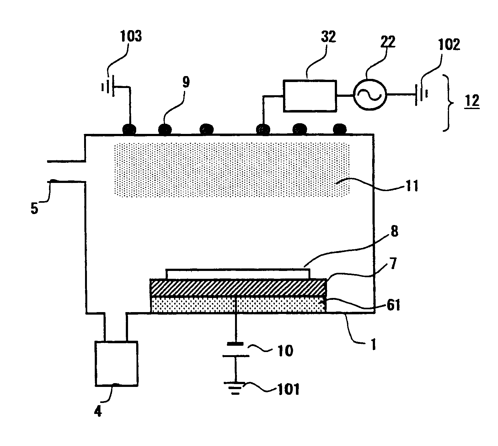
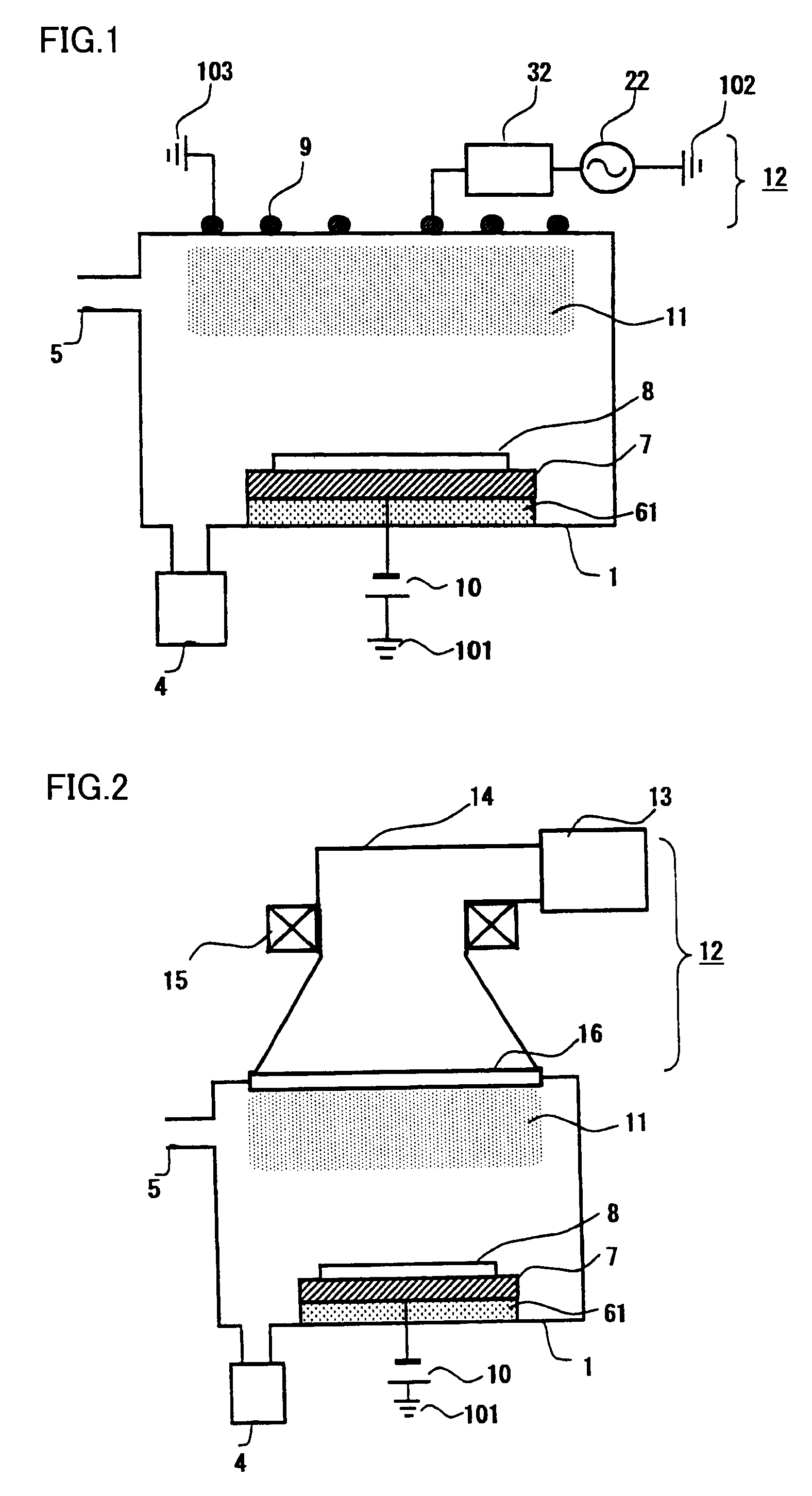
[0017]FIG. 1 is a schematic view that shows a schematic structure of a plasma CVD apparatus (hereinafter, referred to as a PCVD apparatus) in accordance with Embodiment 1 of the present invention. As shown in FIG. 1, the PCVD apparatus in accordance with the present invention is provided with a reaction chamber having a vacuum pump 4 and a material inlet 5 used for supplying a compound having a borazine skeleton, a feeding electrode 7 that is installed in reaction chamber 1 to support a substrate 8, and that is applied with a negative charge, and a plasma generator 12 that is arranged opposite to feeding electrode 7 via substrate 8 so as to generate a plasma 11 within reaction chamber 1.

[0018]In the PCVD apparatus of the present invention, a compound having a borazine skeleton is introduced into reaction chamber 1, with a plasma being generated within reaction chamber 1 by plasma generator 12 placed opposite to feeding electrode 7, so that the compound is excited, and by further app...

embodiment 2

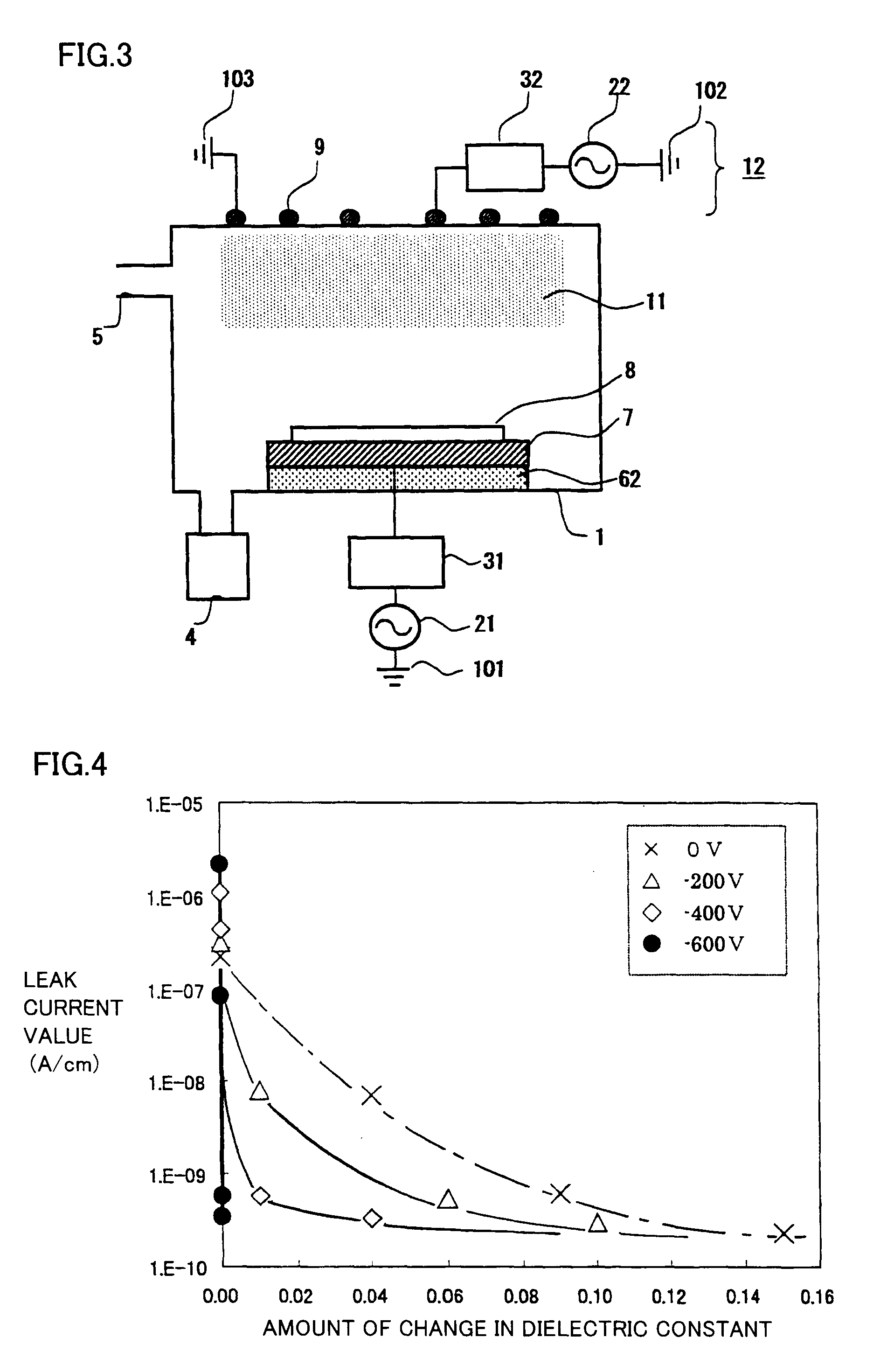
[0034]The following description will discuss a film-forming process in which the PCVD apparatus in accordance with Embodiment 1 is used. First, substrate 8 is placed on feeding electrode 7, and the inside of reaction chamber 1 is vacuum-drawn. Next, a material gas (a compound having a borazine skeleton), a carrier gas and other gases, if necessary, are supplied into reaction chamber 1 through gas inlet 5. Moreover, the pressure inside reaction chamber 1 is vacuum-drawn by vacuum pump 4 to be maintained at a predetermined process pressure. Here, substrate 8 is set to a predetermined process temperature by using heating device 61 or heating / cooling device 62.

[0035]Moreover, when a high frequency is generated by high frequency power supply 22 so that plasma 11 is generated inside reaction chamber 1, the material gas (composition having a borazine skeleton) and the carrier gas are formed into ions and radicals in reaction chamber 1. Of these, the ions are drawn by the electrode having a...

embodiment 3

[0042]By using the PCVD apparatus shown in the above-mentioned Embodiment 1, a film formed by the thin-film forming method shown in the above-mentioned Embodiment 2 was used as an insulating layer and a wiring pattern made of copper was formed thereon, and these processes were repeated so that a semiconductor device having several laminated layers was manufactured. FIG. 5 is a schematic cross-sectional view showing one example of the semiconductor device. Insulating films 502 and 509, a first insulating layer 503, a second insulating layer 505 and a third insulating layer 507 were formed by using the PCVD apparatus shown in the above-mentioned Embodiment 1 through the thin-film forming method in accordance with the above-mentioned Embodiment 2. In the above-mentioned semiconductor device, it was confirmed that wiring delay could be reduced in comparison with the structure in which the insulating layers were made from silicon oxide or silicon nitride. Moreover, it was also confirmed ...


PUM

PropertyMeasurementUnit
poweraaaaaaaaaa
voltageaaaaaaaaaa
dielectric constantaaaaaaaaaa

Abstract

A plasma CVD apparatus including a reaction chamber including an inlet for supplying a compound including a borazine skeleton, a feeding electrode, arranged within the reaction chamber, for supporting a substrate and being applied with a negative charge, and a plasma generating mechanism, arranged opposite to the feeding electrode via the substrate, for generating a plasma within the reaction chamber. A method forms a thin film wherein a thin film is formed by using a compound including a borazine skeleton as a raw material, and a semiconductor device includes a thin film formed by such a method as an insulating film. The apparatus and method enable to produce a thin film wherein low dielectric constant and high mechanical strength are stably maintained for a long time and insulating characteristics are secured.

Description

TECHNICAL FIELD[0001]The present invention relates to a plasma CVD (Chemical Vapor Deposition) apparatus that forms a thin film by using a compound having a borazine skeleton as a raw material. The present invention also relates to a thin-film forming method for forming a thin film by using such a compound having a borazine skeleton as a raw material. Moreover, the present invention relates to a semiconductor device that is provided with a thin film formed by this thin-film forming method as an insulating film.BACKGROUND ART[0002]Along with the developments of high-speed and highly integrated semiconductor devices, a signal delay has caused a serious problem. The signal delay is represented by the product of the resistance value of wiring and the capacity between wirings as well as between layers, and in order to suppress the signal delay to the minimum, effective methods are to reduce the wiring resistance and also to lower the dielectric constant of an interlayer insulating film.[...

Claims


Application Information

Patent Timeline
Patent Type & Authority Patents(United States)
IPC IPC(8): C23C8/00H01L23/58
CPCC23C16/30C23C16/342C23C16/511H01J37/32532H01L21/318B05D1/62H01L21/02274H01L21/02205H01L21/02112H01L21/205
Inventor KUMADA, TERUHIKONOBUTOKI, HIDEHARUYASUDA, NAOKI
Owner MITSUBISHI ELECTRIC CORP
Why Eureka
Try Eureka