
Low temperature wafer level processing for MEMS devices

a technology of mems devices and wafers, which is applied in the direction of fluid pressure measurement, fluid pressure measurement by electric/magnetic elements, instruments, etc., can solve the problems of small damping of mechanical structure vibration, difficult to gear up the mems fabrication process to general applications, and inability to meet the requirements of general applications

Active Publication Date: 2013-04-02
MCGILL UNIV
View PDF15 Cites 7 Cited by
  • Summary
  • Abstract
  • Description
  • Claims
  • Application Information

AI Technical Summary

Benefits of technology

The patent describes a method for making a microelectromechanical systems (MEMS) device on a substrate. The method includes creating a cavity in the substrate, filling it with a material, and using an invention called a via to electrically connect the MEMS device to other components on the substrate. The method also includes adding a metallization to the via, creating an electrical contact pad, and fabricating a MEMS device on the second surface of the substrate. The technical effects of the patent include improving the reliability and performance of MEMS devices, reducing the size and cost of devices, and simplifying the manufacturing process.

Problems solved by technology

Indeed, reduced pressure minimizes air resistance, resulting in smaller damping of the mechanical structure's vibration.
However, because of this vast range of functionality, MEMS fabrication processes, unlike the microelectronics industry, are difficult to gear towards general applications.
As a result, most processes are aimed at the fabrication of a few devices, and usually performance of the devices is hindered by process variability.
For all its widespread use, chip-level packaging (CLP) presents significant drawbacks that make it particularly costly, including:1) Very expensive hermetically sealable packages are required;2) The chips must be encapsulated individually rather than by means of a batch process.
This lengthens the production time of the system, thereby increasing costs;3) The fragile MEMS devices are not protected during dicing and wire bonding, which has a negative impact on the yield, thus incurring greater costs; and4) For many systems, e.g. radio frequency integrated circuits, the CLP solution introduces capacitive and inductive parasitic elements which can be detrimental to performance, thus requiring additional potentially costly remedies.
In fact, the costs of using CLP for hermetical packaging can exceed any other costs involved in the design of a MEMS system.
However, the external package is neither responsible for hermetically preserving a vacuum environment nor ensuring the fine mechanical protection of the MEMS devices: all this is performed by the WLP encapsulation.
With CLP, expensive enclosures are wasted to test faulty devices, since each die must be fully packaged before it can be verified.
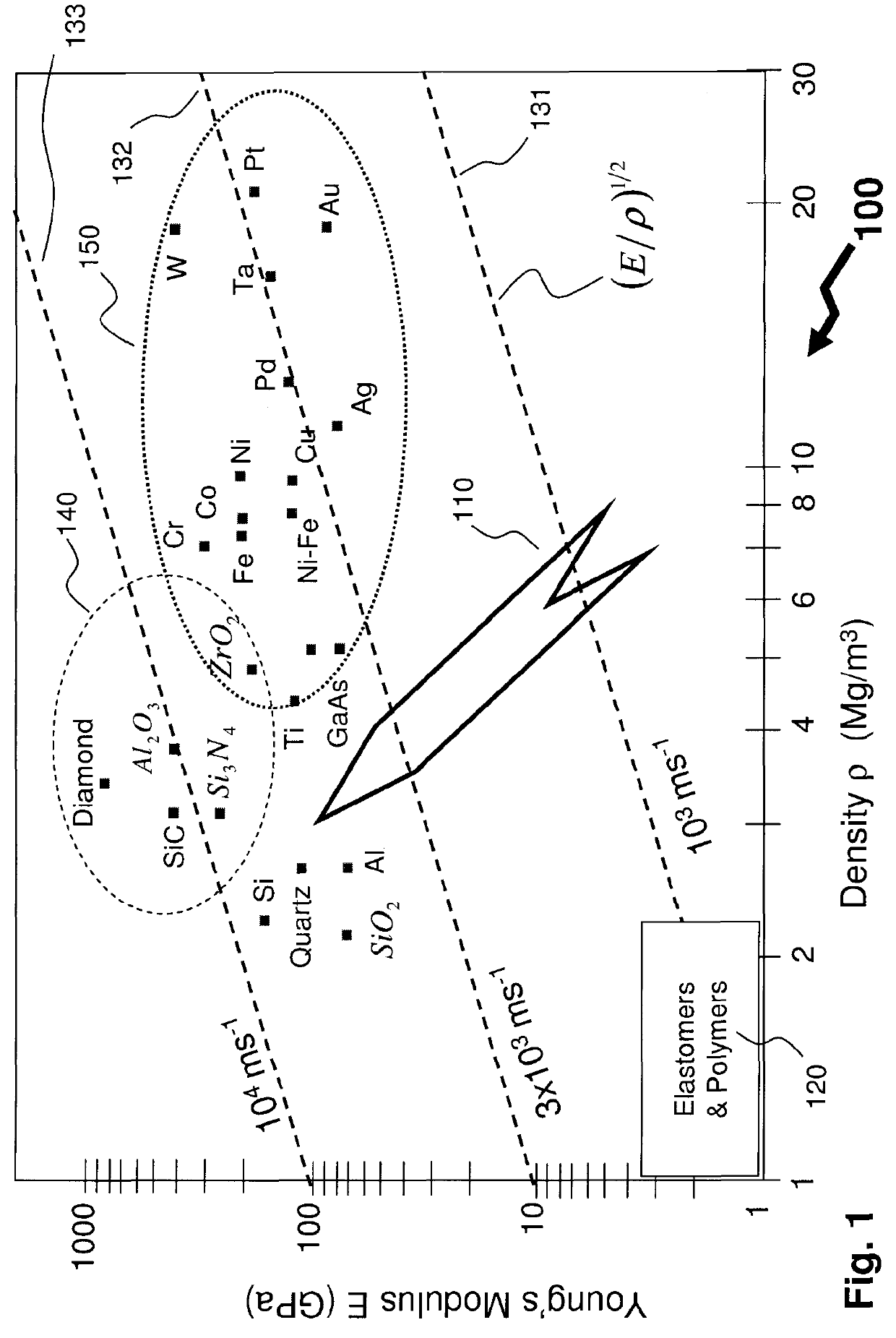
Within the prior art the vast majority of research and current commercial products has been undertaken on silicon due to the availability of a manufacturing and process infrastructure from electronics However, the mechanical properties of silicon do not make it the most suitable structural material for MEMS.
However, difficulties with SiC processing have made its use non-trivial as it is non-conductive and difficult to deposit and dope at temperatures compatible with CMOS electronics.
Stress control is also difficult because of the high intrinsic stresses that can develop in such a material.
Because of its intrinsic inertness, selective etching of SiC is difficult.
As most materials are etched at a faster rate than SiC, issues arise when masking SiC for patterning and ensuring a reliable etch-stop.
As such prior art SiC MEMS processes have not lent themselves well to CMOS integration.
Such an interconnection that would traverse through the wafer bonding interface between the silicon substrate and the cover wafer providing the hermetic seal, and cause topography and sealing issues, as well as performance issues due to parasitics.
However, the provisioning of vertical feed-throughs through the thickness of the substrate provides two drawbacks within the prior art.
Such membranes form one potential point of failure for the packaged component due to rupturing, gas transport, etc.
Secondly the removal of large portions of the silicon substrate beneath the MEMS device results in a weakening of the mechanical integrity and impacts the performance of the MEMS device.

Method used


Image

  • Low temperature wafer level processing for MEMS devices
  • Low temperature wafer level processing for MEMS devices
  • Low temperature wafer level processing for MEMS devices

Examples


first embodiment

[0106]Referring to FIG. 5 there is depicted the invention as applied to the provisioning of SiC mechanical structure 500 with ceramic reinforced wafer electrical feed-throughs forming part of a silicon wafer 510 with an integrated SiC MEMS device. Accordingly as shown a silicon wafer 510 has through-wafer via interconnects 5000 which have been metalized to form interconnect vias 570 after etching with the deposition of aluminum 403. The through-wafer via interconnects 5000 being aligned with openings 540 within the silicon dioxide 401 on the front surface of the wafer. The through-wafer via interconnects 5000 interconnect to first level metallizations 530A and 530B on the upper surface of the silicon wafer 510.

[0107]Formed upon the first level metallization 530B there is a MEMS structure 520 formed from low temperature ceramic MEMS material 404, such as silicon carbide 407. Within each through-wafer via interconnect 5000 there is deposited a reinforcing barrier 590 from a low temper...

second embodiment

[0109]Referring to FIG. 6 there is depicted the invention as applied to the provisioning of a SiC mechanical structure 600 with ceramic reinforced wafer electrical feed-throughs forming part of a silicon wafer 610 with an integrated device comprising SiC MEMS and CMOS electronics. Accordingly as shown a silicon wafer 610 has through-wafer via interconnects 6000 which have been metalized to form interconnect vias 670 after etching with the deposition of aluminum 403. The through-wafer via interconnects 6000 being aligned with openings 640A and 640B within the silicon dioxide 401 on the front surface of the wafer. The through-wafer via interconnects 6000 interconnect to first level metallizations 630A and 630B on the upper surface of the silicon wafer 610.

[0110]Formed upon the first level metallization 630B there is a MEMS structure 620 formed from low temperature ceramic MEMS material 404, such as silicon carbide 407. Within each through-wafer via interconnect 6000 there is deposited...

third embodiment

[0113]FIG. 7 depicts the invention as applied to the packaging of a MEMS device 780 manufactured onto a silicon circuit with integrated CMOS electronics wherein the resultant package is mounted to a PCB 770. Accordingly as shown the MEMS device 780, such as SiC mechanical structure 600 of FIG. 6 supra, has been hermetically packaged with a lid 710. Lid 710 having been manufactured with a getter material 720. The solder infill 790 of the through-wafer electrical vias, such as through-wafer via interconnect 6000 of FIG. 6, are electrically connected to PCB metallization 730. The PCB 770 supports through-PCB vias 750 which terminate in solder bump interconnect 760, and direct mounting of integrated circuits, represented by generic IC package 740. Said ancillary integrated circuits providing functions such as power supply generation, signal conditioning, signal processing, and digital communications. This embodiment reduces the interconnect parasitics with the PCB over traditional packa...


PUM


Abstract

Microelectromechanical systems (MEMS) are small integrated devices or systems that combine electrical and mechanical components. It would be beneficial for such MEMS devices to be integrated with silicon CMOS electronics and packaged in controlled environments and support industry standard mounting interconnections such as solder bump through the provisioning of through-wafer via-based electrical interconnections. However, the fragile nature of the MEMS devices, the requirement for vacuum, hermetic sealing, and stresses placed on metallization membranes are not present in packaging conventional CMOS electronics. Accordingly there is provided a means of reinforcing the through-wafer vias for such integrated MEMS-CMOS circuits by in filling a predetermined portion of the through-wafer electrical vias with low temperature deposited ceramic materials which are deposited at temperatures below 350° C., and potentially to below 250° C., thereby allowing the re-inforcing ceramic to be deposited after fabrication of the CMOS electronics.

Description

CROSS-REFERENCE TO RELATED APPLICATIONS[0001]This application claims the benefit of priority to U.S. Provisional Patent Application Ser. No. 61 / 064,534 filed Mar. 11, 2008 entitled “Low Temperature Wafer Level Packaging for MEMS Devices” and U.S. Provisional Patent Application Ser. No. 61 / 129,909 filed Jul. 29, 2008 entitled “Low Temperature Wafer Level Packaging for MEMS Devices”FIELD OF THE INVENTION[0002]The invention relates to the processing of microelectromechanical devices (MEMS) and more particularly to providing structural elements within said MEMS devices and the substrates upon which they are manufactured.BACKGROUND OF THE INVENTION[0003]Microelectromechanical systems (MEMS) are small integrated devices or systems that combine electrical and mechanical components. The components can range in size from the sub-micrometer level to the millimeter level, and there can be any number, from one, to few, to potentially thousands or millions, in a particular system. Historically M...

Claims


Application Information

Patent Timeline
Patent Type & Authority Patents(United States)
IPC IPC(8): H01L21/768H10N30/00
CPCG01L9/0042H01L21/76898H01L23/481H01L2924/12044H03H3/007H03H9/10H01L2224/131H01L2224/0557H01L2224/13009H01L2224/13021H01L2224/13023H01L2924/1461H01L2924/00014H01L2924/0002H01L2224/0401B81C1/00301H01L2924/014H01L2924/00H01L2224/05552H01L21/02697
Inventor EL-GAMAL, MOURADLEMOINE, DOMINIQUECICEK, PAUL-VAHENABKI, FREDERIC
Owner MCGILL UNIV
Learn More