Embedded NOR flash memory process with NAND cell and true logic compatible low voltage device

a technology of embedded flash memory and nand cell, which is applied in the direction of semiconductor devices, semiconductor/solid-state device details, electrical devices, etc., can solve the problems of low application compatibility, low application compatibility, and low read speed of nand flash memory, so as to limit the extent of depletion regions

Inactive Publication Date: 2013-06-04
APLUS FLASH TECH
View PDF28 Cites 9 Cited by
  • Summary
  • Abstract
  • Description
  • Claims
  • Application Information

AI Technical Summary

Benefits of technology

[0015]The nonvolatile memory array circuits are constructed of rows and columns of NAND or NOR charge retaining cells formed within designated active areas. The NOR charge retaining cells are NAND-based NOR memory cells having at least two floating gate transistors serially connected such that at least one of the floating gate transistors functions as a select gate transistor to prevent leakage current through the charge retaining transistors when the charge retaining transistors is not selected for reading. The nonvolatile memory array circuits formed of NAND-based NOR charge retaining cells has a column of the NAND-based NOR charge retaining cells with a bit line and source line associated with each column of the NAND-based NOR charge retaining cells. A drain of the topmost charge retaining transistor is connected to the bit line associated with and parallel to each of the columns of serially connected NAND-based NOR charge retaining cells. Similarly, a source of the bottommost charge retaining transistor is connected to the source line associated with and parallel to each of the columns of NAND-based NOR charge retaining cells and parallel to the associated bit line. A control gate of each of the rows of NAND-based NOR flash memory cells is connected to a word line.
[0020]An active area mask is employed to define the areas of the shallow trench isolation to separate the area of the nonvolatile memory array circuits, the logic circuits and the linear analog circuits. The defined areas of the active area mask are etched to create the trenches and then filled with trench insulation that in various embodiments is a silicon oxide. Further, in various embodiments the shallow trench isolation self-aligns the charge retaining regions of the charge retaining transistors. In the embodiments having floating gate charge retaining regions, the shallow trench isolation provides the self alignment of the first conductive layer to improve performance of the charge retaining transistors.
[0022]A second conductive layer is formed on the surface of the substrate. In various embodiments, the conductive layer is a second polycrystalline silicon that is deposited to thickness of from approximately 1,500 Å to 3,000 Å. The second polycrystalline silicon conductive layer is doped to with an impurity to increase the conductivity of the second polycrystalline silicon conductive layer. In some embodiments, the second polycrystalline silicon conductive layer has a conductive film added to a top surface to form a low resistance polycide layer. A capping layer is deposited over the second conductive layer to prevent peeling of the conductive films where in various embodiments the conductive films are tungsten.
[0025]A peripheral implant mask is formed over the substrate leaving the nonvolatile memory array circuits exposed for a cell source and drain implant. The stacked gate is self-aligning feature for the cell source / drain implant of the first conductivity type to form the source and drains for the charge retaining transistors. In some embodiments, the cell source / drain implant is preceded by a halo implant of the second conductivity type within the triple well against the junction walls to limit the extent of depletion regions.

Problems solved by technology

This leakage current is sufficient large to cause the consumption of a relatively large amount of power during programming.
However, NAND flash memory has a relatively slow read speed and is thus not suitable for an embedded application.
While there are embedded NAND and NOR flash memory designs, there is no true embedded flash memory technology that is available for mass production in the semiconductor industry that has low power consumption to meet the requirement of “Green Memory”.

Method used


Image

  • Embedded NOR flash memory process with NAND cell and true logic compatible low voltage device
  • Embedded NOR flash memory process with NAND cell and true logic compatible low voltage device
  • Embedded NOR flash memory process with NAND cell and true logic compatible low voltage device

Examples


Embodiment Construction

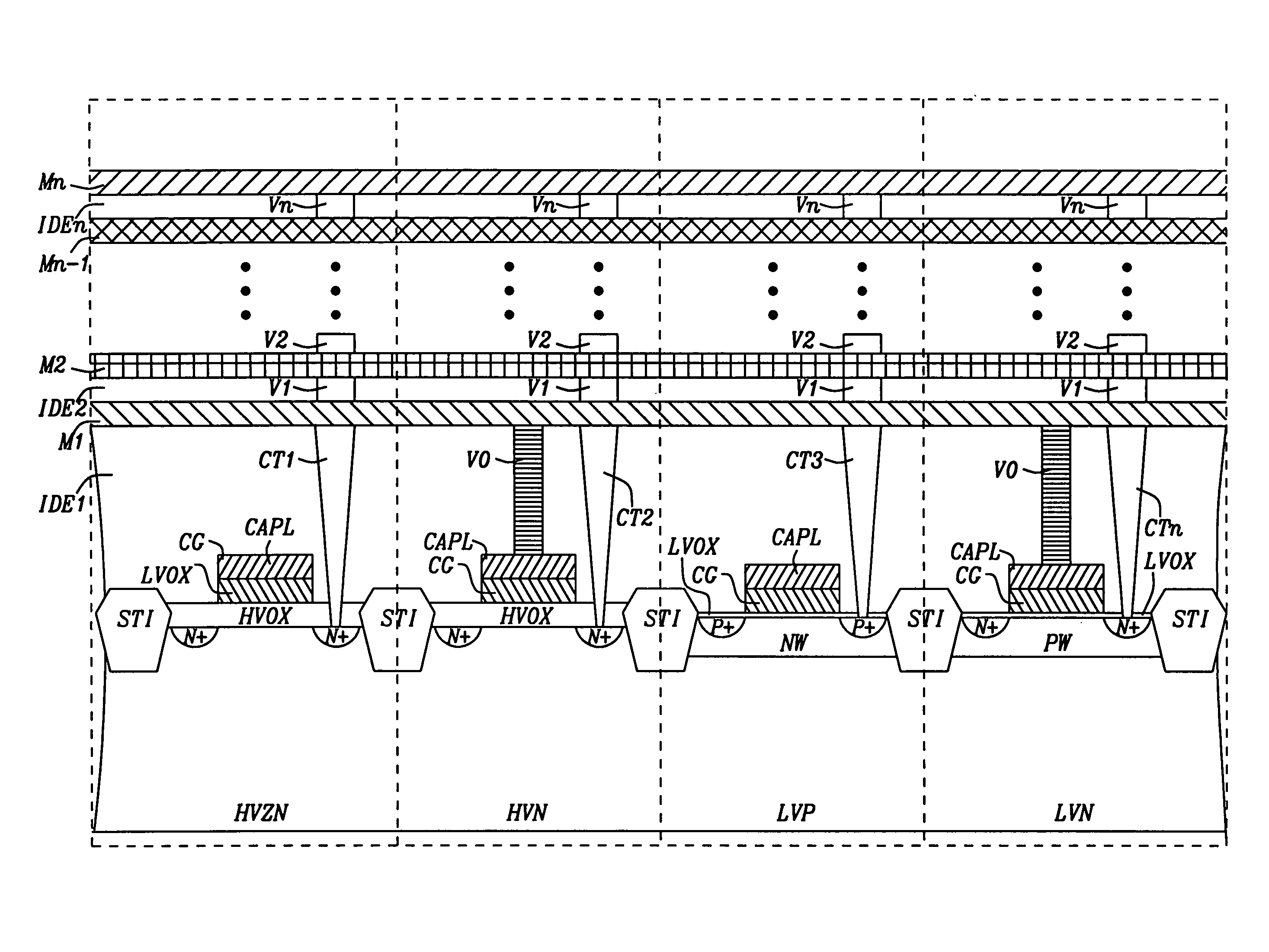
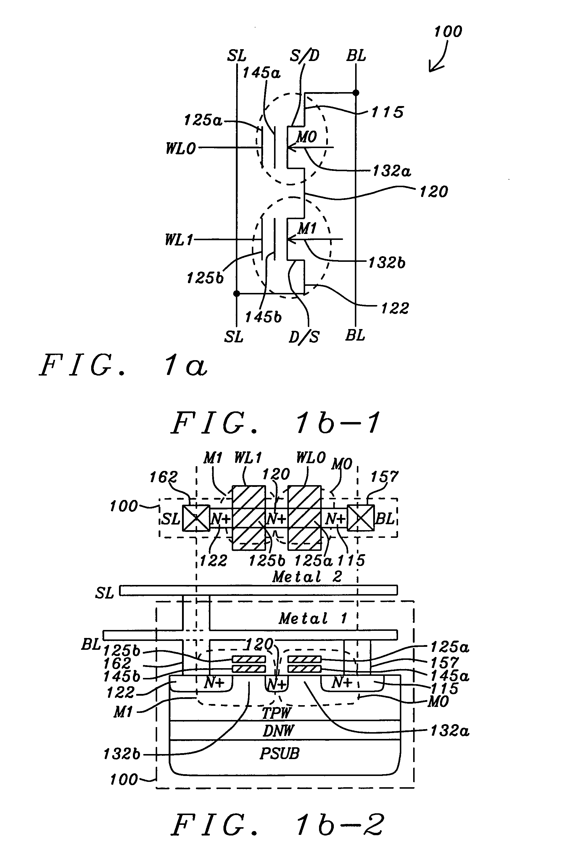
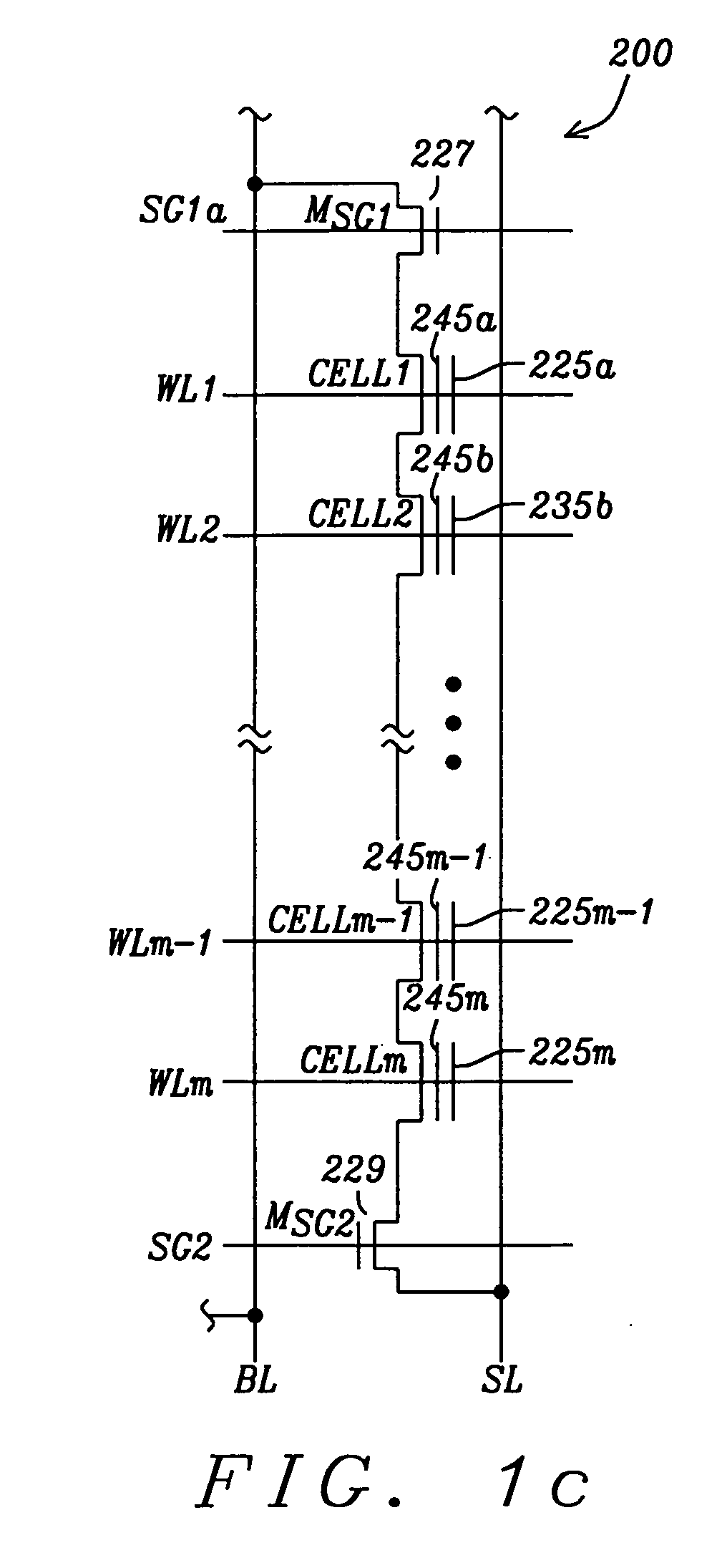
[0038]The punch-through phenomenon of the charge retaining transistors of the NOR flash memory cell has forced the charge retaining transistors to be fabricated with a sufficiently large channel length to prevent the punch-through. While the NAND flash memory cell is structured to have a serial NAND string with a gating transistor that overcomes the scaling problem, the NAND flash memory cell has a relatively slow read speed. The size of the NOR flash memory cell and the slow read speed of the NAND flash memory cell make them actually unsuitable embedded flash memory technology for System-on-Chip (SoC) designs. The power consumption of the NOR flash memory cells of the prior art does not meet the requirements of “Green Memory”. The slow read speed of the NAND cell can not meet the performance requirements for SoC designs.

[0039]The 771 patent application describes a NAND-based NOR flash memory cell. The NAND-based NOR memory cell is designed and marketed by APlus Flash Technology, In...


PUM


Abstract

An integrated circuit formed of nonvolatile memory array circuits, logic circuits and linear analog circuits is formed on a substrate. The nonvolatile memory array circuits, the logic circuits and the linear analog circuits are separated by isolation regions formed of a shallow trench isolation. The nonvolatile memory array circuits are formed in a triple well structure. The nonvolatile memory array circuits are NAND-based NOR memory circuits formed of at least two floating gate transistors that are serially connected such that at least one of the floating gate transistors functions as a select gate transistor to prevent leakage current through the charge retaining transistors when the charge retaining transistors is not selected for reading. Each column of the NAND-based NOR memory circuits are associated with and connected to one bit line and one source line.

Description

[0001]This application claims priority under 35 U.S.C. §119 to U.S. Provisional Patent Application Ser. No. 61 / 398,964, filed on Jul. 1, 2010, assigned to the same assignee as the present invention, and incorporated herein by reference in its entirety.RELATED PATENT APPLICATIONS[0002]U.S. patent application Ser. No. 12 / 387,771 (771), filed on May 7, 2009 assigned to the same assignee as the present invention, and incorporated herein by reference in its entirety.[0003]U.S. patent application Ser. No. 12 / 455,337, filed on Jun. 1, 2009 assigned to the same assignee as the present invention, and incorporated herein by reference in its entirety.[0004]U.S. patent application Ser. No. 12 / 455,936, filed on Jun. 9, 2009 assigned to the same assignee as the present invention, and incorporated herein by reference in its entirety.[0005]U.S. patent application Ser. No. 12 / 456,354, filed on Jun. 16, 2009 assigned to the same assignee as the present invention, and incorporated herein by reference ...

Claims


Application Information

Patent Timeline
Patent Type & Authority Patents(United States)
IPC IPC(8): H01L27/118
CPCH01L27/11526H01L27/11546H01L29/66825H01L29/7881H01L27/115H10B41/49H10B41/40H10B69/00
Inventor LEE, PETER WUNGMA, HAN-REIHSU, FU-CHANG
Owner APLUS FLASH TECH
Why Eureka
Try Eureka