Method for etching single wafer
a single-wallet etching technology, applied in the field of methods, can solve the problems of affecting the etching effect of the etching amount is not enough, so as to improve the degree of freedom to control the distribution of etching amount on the surface of the wafer, improve the etching effect, and improve the effect of etching
- Summary
- Abstract
- Description
- Claims
- Application Information
AI Technical Summary
Benefits of technology
Problems solved by technology
Method used
Image
Examples
example 1
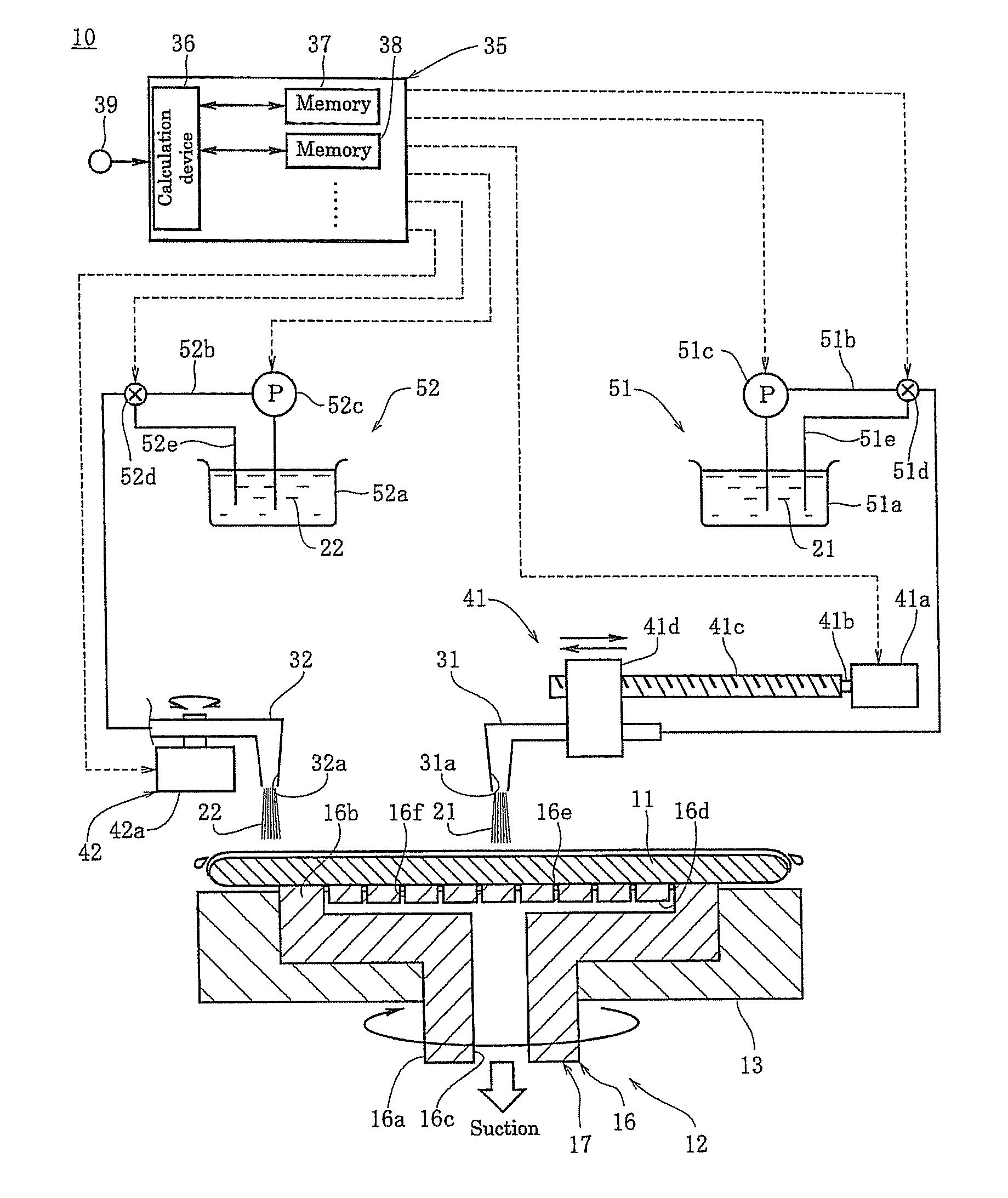
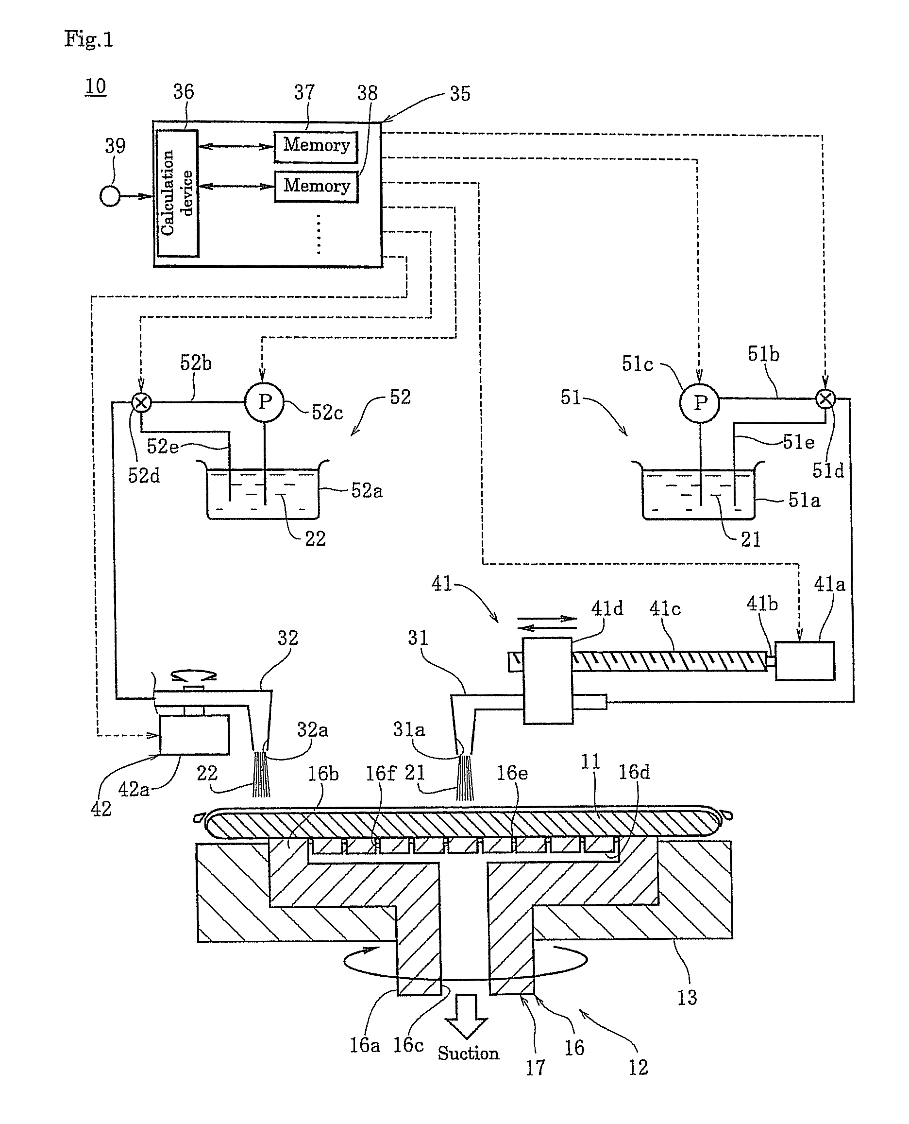
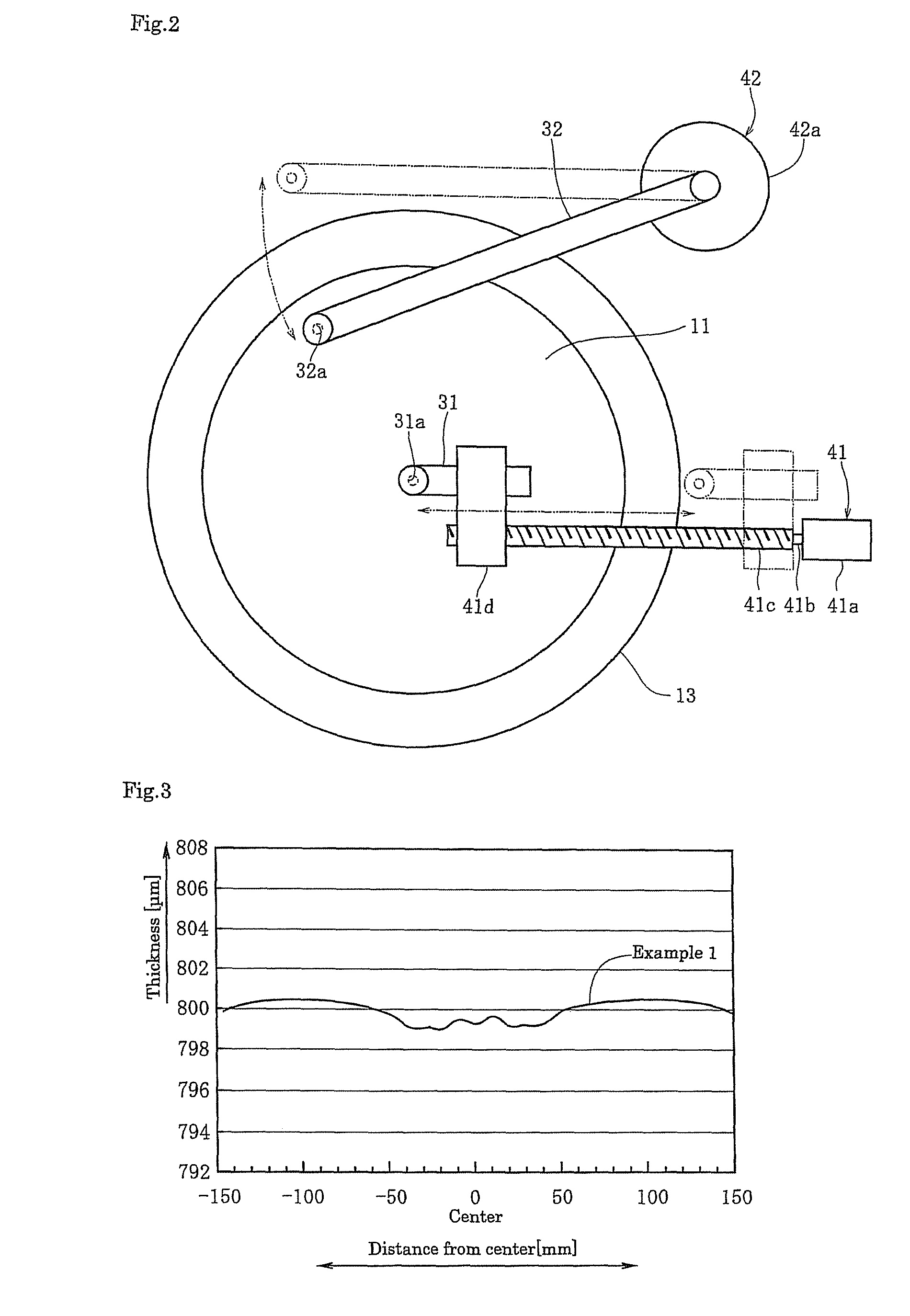
[0045]As shown in FIGS. 1 and 2, a wafer obtained by slicing a silicon single crystal ingot was subjected to chamfering and mechanical grinding (lapping), so that there was also prepared a silicon wafer 11 of 300 mm in diameter of which front and back surfaces were flattened. In addition, a first etching solution 21 was prepared by mixing an aqueous hydrofluoric acid solution at a weight concentration of 50%, an aqueous nitric acid solution at a weight concentration of 70%, and an aqueous phosphoric acid solution at a weight concentration of 85% in a volume ratio of 4:7.4:6 and then reserved in a first tank 51a heated at 30° C. On the other hand, a second etching solution 22 was prepared by mixing 50% by weight concentration of an aqueous fluorine acid solution, 70% by weight concentration of an aqueous nitric acid solution, and 80% by weight concentration of an aqueous phosphoric acid solution in a volume ratio of 4:7.4:6 and then reserved in a second tank 52a heated at 20° C. Unde...
example 2
[0046]Etching of wafer was carried out by the same way as that of Example 1, except that a second etching solution used was an etching solution prepared by mixing an aqueous hydrofluoric acid solution at a weight concentration of 50%, an aqueous nitric acid solution at a weight concentration of 70%, and an aqueous phosphoric acid solution at a weight concentration of 85% at a volume ratio of 3:8:6 and then kept at a temperature of 30° C. Therefore, the etched wafer was provided for Example 2.
example 3
[0047]Etching of wafer was carried out by the same way as that of Example 1, except that the second etching solution was supplied from the second supply nozzle onto the periphery of the front surface of the wafer at a flow rate of 3 l / min. Therefore, the etched wafer was provided for Example 3.
PUM
| Property | Measurement | Unit |
|---|---|---|
| temperature | aaaaa | aaaaa |
| temperature | aaaaa | aaaaa |
| temperature | aaaaa | aaaaa |
Abstract
Description
Claims
Application Information


