Asymmetric static random access memory cell with dual stress liner

a random access memory and stress liner technology, applied in the field of solid-state memory, can solve the problems of increasing the probability of read and write functional failures, physical scaling of device sizes, and increasing the variability of electrical characteristics, so as to improve the static noise margin

Active Publication Date: 2013-06-18
TEXAS INSTR INC
View PDF12 Cites 18 Cited by
  • Summary
  • Abstract
  • Description
  • Claims
  • Application Information

AI Technical Summary

Benefits of technology

[0021]Embodiments of this invention provide a memory cell, and method of constructing the same, in which static noise margin is improved without requiring increase in chip area.
[0022]Embodiments of this invention provide such a memory cell and method in which static noise margin is improved in a cost-free manner, from the standpoint of manufacturing cost.
[0023]Embodiments of this invention provide such a memory cell and method in which static noise margin is improved without requiring changes to circuit design.

Problems solved by technology

However, this physical scaling of device sizes raises significant issues, especially in connection with embedded SRAM but also in SRAM realized as “stand-alone” memory integrated circuit devices.
Several of these issues are due to increased variability in the electrical characteristics of transistors formed at these extremely small feature sizes.
This variability in characteristics has been observed to increase the likelihood of read and write functional failures, on a cell-to-cell basis.
The combination of increased device variability with the larger number of memory cells (and thus transistors) within an integrated circuit renders a high likelihood that one or more cells cannot be read or written as expected.
As mentioned above, device variability can cause read and write failures, particularly in memory cells constructed with sub-micron minimum feature size transistors.
A write failure occurs when an addressed SRAM cell does not change its stored state when written with the opposite data state.
Typically, this failure has been observed to be due to the inability of write circuitry to pull down the storage node currently latched to a high voltage.
Cell stability failures are the converse of write failures—a write failure occurs if a cell is too stubborn in changing its state, while a cell stability failure occurs if a cell changes its state too easily, such as may occur to a memory cell in a selected row but an unselected column (i.e., a “half-selected” cell) during a write to a cell in a selected column in its same row.
Noise of sufficient magnitude coupling to the bit lines of the half-selected columns, during a write to the selected columns in the same row, can cause a false write of data to those half-selected columns.
The possibility of such stability failure is exacerbated by device mismatch and variability, as discussed above.
Unfortunately, the design window in which both adequate cell stability and adequate write margin can be attained is becoming smaller with continued scaling-down of device feature sizes, for the reasons mentioned above.
In addition, it has been observed that the relative drive capability of p-channel MOS transistors relative to re-channel MOS transistors is increasing as device feature sizes continue to shrink, which skews the design window toward cell stability over write margin.
However, in an interleaved architecture, half-selected cells in a write cycle (i.e., cells in the selected row that are not being written) can still exhibit cell instability, because the write word line will be energized in that situation.
As known in the art, non-interleaved memory arrays are vulnerable to multiple-bit soft error failures, and consume additional chip area.

Method used


Image

  • Asymmetric static random access memory cell with dual stress liner
  • Asymmetric static random access memory cell with dual stress liner
  • Asymmetric static random access memory cell with dual stress liner

Examples


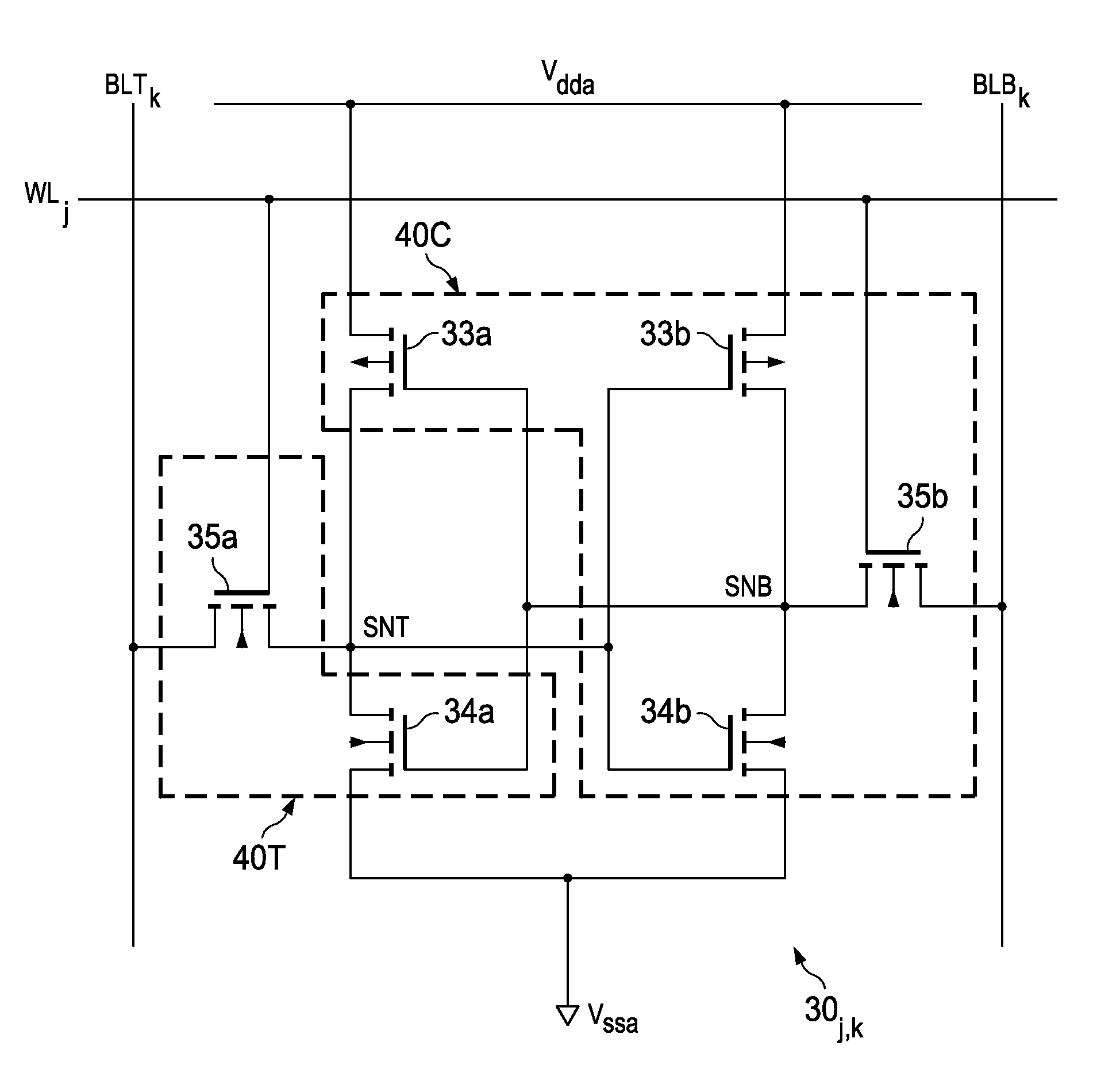
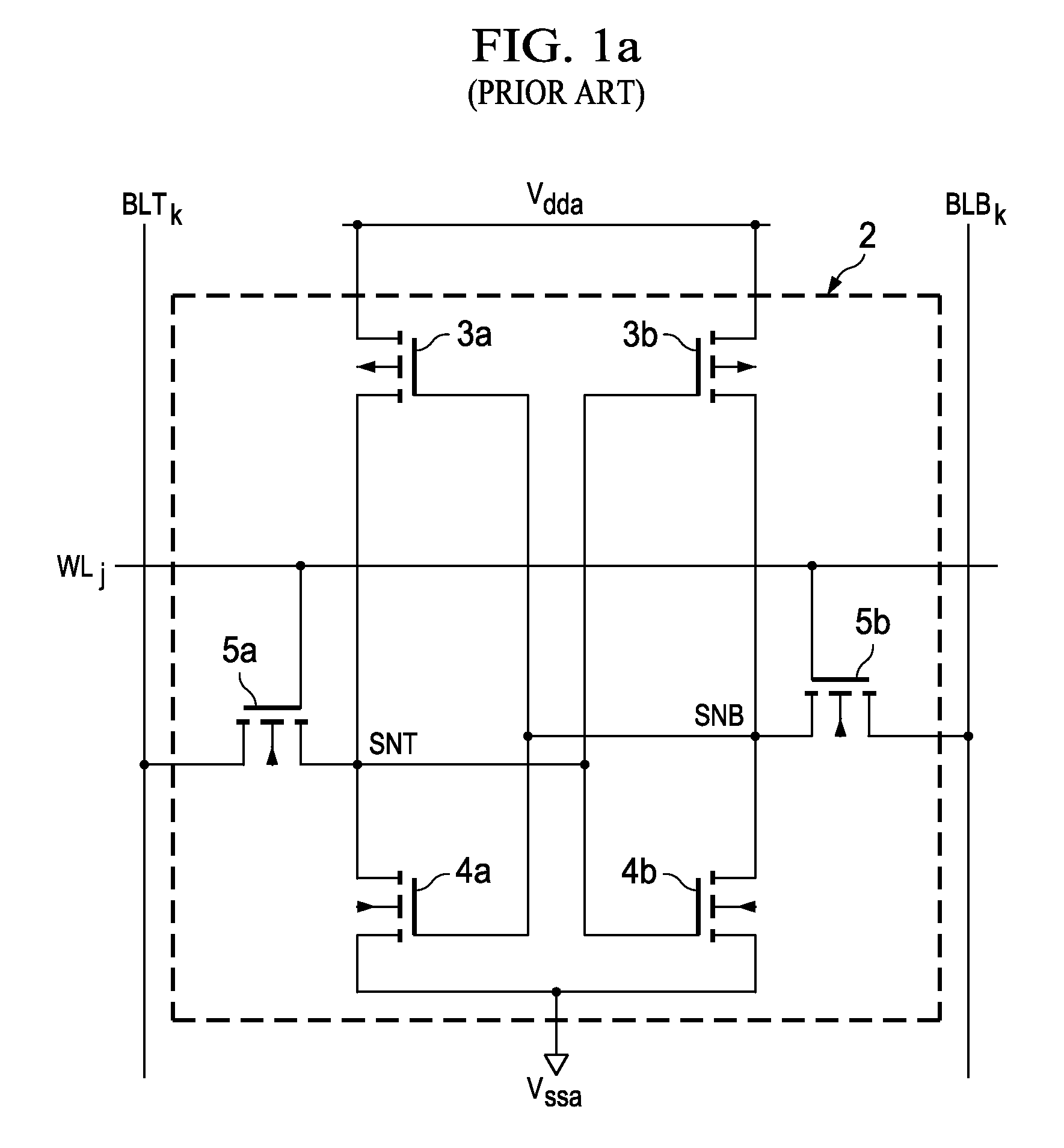
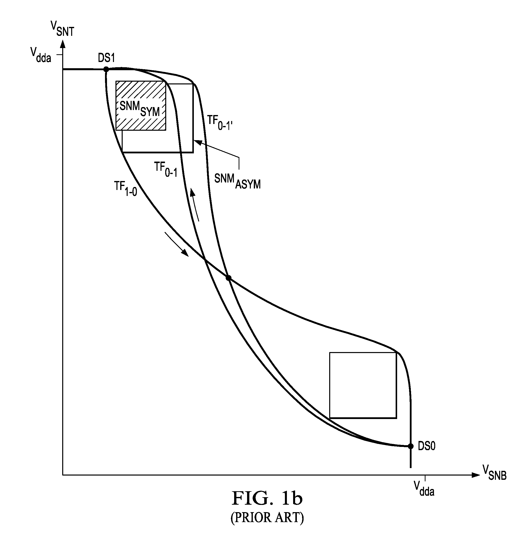
Embodiment Construction

[0040]The present invention will be described in connection with its embodiments, namely as implemented into a static random access memory (SRAM) embedded within a larger scale integrated circuit, and constructed according to complementary metal-oxide-semiconductor (CMOS) technology, because it is contemplated that this invention is especially beneficial in such an application. However, it is contemplated that those skilled in the art having reference to this specification will readily recognize that this invention may be applied to a wide range of memory devices. Accordingly, it is to be understood that the following description is provided by way of example only, and is not intended to limit the true scope of this invention as claimed.

[0041]FIG. 2 illustrates an example of large-scale integrated circuit 10, in the form of a so-called “system-on-a-chip” (“SoC”), as now popular in many electronic systems. Integrated circuit 10 is a single-chip integrated circuit into which an entire...


PUM


Abstract

A solid-state memory in which each memory cell is constructed of complementary metal-oxide-semiconductor (CMOS) inverters implemented with dual stress liner (DSL) technology. Asymmetry is incorporated into each memory cell by constructing one of the inverter transistors or the pass-gate transistor using the stress liner with opposite stress characteristics from its opposing counterpart. For example, both of the p-channel load transistors and one of the n-channel driver transistors in each memory cell may be constructed with a compressive nitride liner layer while the other driver transistor is constructed with a tensile nitride liner layer. In another implementation, one of the n-channel pass-gate transistors is constructed with a compressive nitride liner layer while the other pass-gate transistor is constructed with a tensile nitride liner layer. Improved cell stability due to the resulting asymmetric behavior is implemented in a cost-free manner.

Description

CROSS-REFERENCE TO RELATED APPLICATIONS[0001]Not applicable.STATEMENT REGARDING FEDERALLY SPONSORED RESEARCH OR DEVELOPMENT[0002]Not applicable.BACKGROUND OF THE INVENTION[0003]This invention is in the field of solid-state memory. Embodiments of this invention are more specifically directed to static random access memory (SRAM) cells and devices.[0004]Many modern electronic devices and systems now include substantial computational capability for controlling and managing a wide range of functions and useful applications. The computational power of these modern devices and systems is typically provided by one or more processor “cores”. These processor cores operate as a digital computer, in general retrieving executable instructions from memory, performing arithmetic and logical operations on digital data retrieved from memory, and storing the results of those operations in memory. Other input and output functions for acquiring and outputting the data processed by the processor cores ...

Claims


Application Information

Patent Timeline
Patent Type & Authority Patents(United States)
IPC IPC(8): G11C11/00
CPCG11C11/412H01L29/7843H01L27/1104H01L21/823807H01L27/0207H10B10/12
Inventor YU, SHAOFENGLOH, WAH KIT
Owner TEXAS INSTR INC
Why Eureka
Try Eureka