
Heat transfer film, semiconductor device, and electronic apparatus

a technology of heat transfer film and semiconductor device, which is applied in the direction of lighting and heating apparatus, semiconductor/solid-state device details, natural mineral layered products, etc., can solve the problems of reducing the size of the device, difficult to cool a portable device with a small space, and difficult to transfer a sufficient amount of heat, etc., to achieve effective transfer of heat generated, small thickness, and high thermal conductivity

Active Publication Date: 2013-07-02
FURUKAWA ELECTRIC CO LTD
View PDF12 Cites 7 Cited by
  • Summary
  • Abstract
  • Description
  • Claims
  • Application Information

AI Technical Summary

Benefits of technology

This patent describes a heat transfer layer made of carbon and a strain relaxation layer made of a different material that helps to improve heat conductivity in the in-plane direction. This layered structure can efficiently radiate and transport heat from one location to another, making it useful in small-sized semiconductor devices and cooling portable devices like phones.

Problems solved by technology

Accordingly, it is difficult to reduce a size of a device with the heat transfer module, thereby making it difficult to cool a portable device with a small space.
Accordingly, it is difficult to transfer a sufficient amount of heat.
Further, heat tends to dissipate or diffuse in the heat transfer process, thereby causing a harmful effect on the device.
Accordingly, it is difficult to substantially improve the thermal conductivity.

Method used


Image

  • Heat transfer film, semiconductor device, and electronic apparatus
  • Heat transfer film, semiconductor device, and electronic apparatus
  • Heat transfer film, semiconductor device, and electronic apparatus

Examples


first embodiment

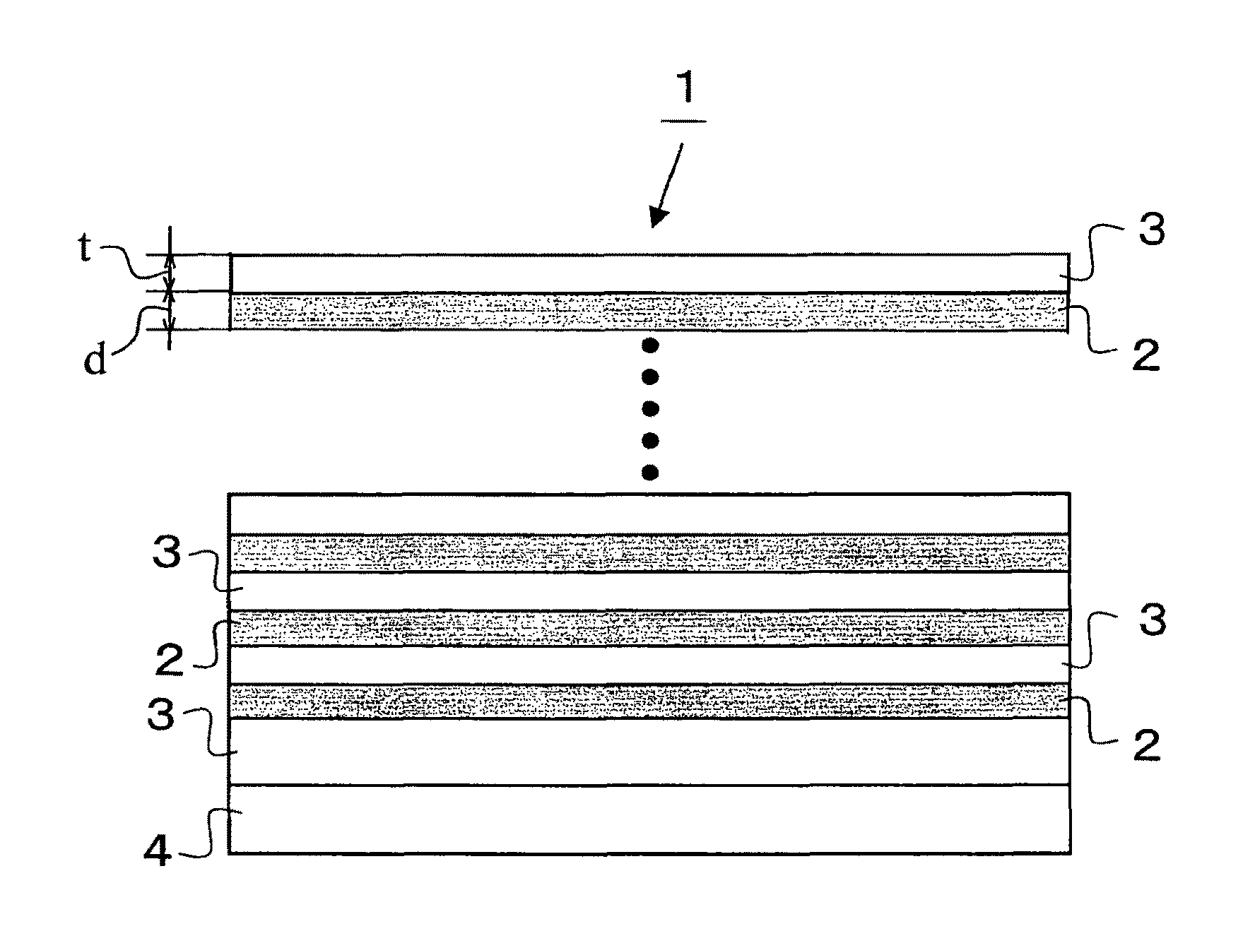
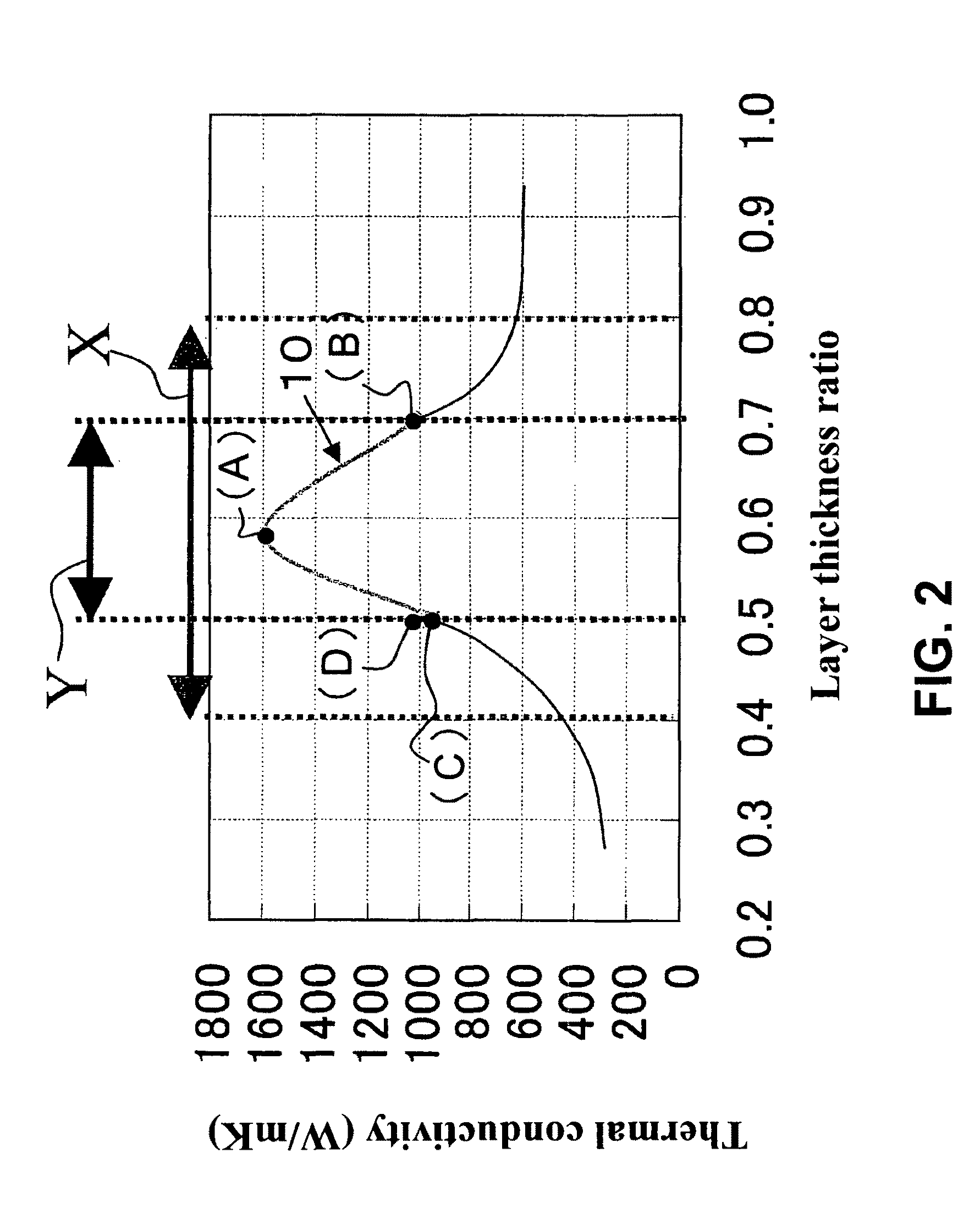
[0072]A first embodiment of the present invention will be described in detail below, based on FIG. 1 to FIG. 5. FIG. 1 is a cross sectional view showing a heat transfer layer according to the first embodiment, FIG. 2 is a graph showing a relation between a layer thickness ratio and a thermal conductivity in in-plane direction, FIG. 3 is a partially enlarged graph of FIG. 2, and FIGS. 4(A) to 4(D) are views showing a mechanism of a heat transfer enhancement by optimizing a configuration of a layer thickness.

[0073]A heat transfer layer 1 as shown in FIG. 1 is configured by stacking a heat transfer layer 2 comprised of a first constituent material as a material including C (carbon) for transferring heat in in-plane direction and a layer thickness direction, and a strain relaxation layer 3 comprised of a second constituent material for relaxing a strain of the first constituent material. Here, a symbol 4 designates a silicon (Si) substrate.

[0074]According to the heat transfer layer 1, a...

second embodiment

[0123]FIG. 5 is a cross sectional view showing a configuration of a semiconductor device according to the second embodiment of the present invention, and FIG. 6 is a cross sectional view showing a configuration of a conventional semiconductor device as a comparative example. Here, a duplicated description is omitted with using a similar symbol for the similar component part regarding FIG. 5 and FIG. 6.

[0124]According to the semiconductor device as shown in FIG. 5, the heat transfer layer 1 as shown in FIG. 1 is formed in the most vicinity of an active layer 21 in an LED (a light emitting diode) chip 20 as a semiconductor light emitting element. More specifically, the heat transfer layer 1 is provided at a peripheral part of a light transmission part 22 existing in the most vicinity of the active layer 21 in the LED chip 20.

[0125]Light emitted from the active layer 21 of the LED chip 20 is transmitted through the light transmission part 22 and then output outward. Here, the silicon s...

third embodiment

[0130]FIG. 7 is a cross sectional view showing a configuration of a semiconductor device according to the third embodiment of the present invention, and FIG. 8 is a cross sectional view showing a configuration of a conventional semiconductor device as a comparative example. Here, a duplicated description is omitted with using a similar symbol for the similar component part regarding FIG. 7 and FIG. 8.

[0131]The semiconductor device as shown in FIG. 7 is configured as a communications laser module, and FIG. 7 shows a part of the communications laser module. In a semiconductor laser diode 30 as a semiconductor light emitting element, the heat transfer layer 1 as shown in FIG. 1 is formed. More specifically, the heat transfer layer 1 is formed in the vicinity of an active layer 31 in the semiconductor laser diode 30 inside. Moreover, a symbol 32 designates an edge face at a light output side regarding edge faces of a resonator, and light generated in the active layer 31 is output from t...


PUM

PropertyMeasurementUnit
thicknessaaaaaaaaaa
thicknessaaaaaaaaaa
thicknessaaaaaaaaaa

Abstract

A heat transfer film includes a heat transfer layer formed of a first constituent material containing C (carbon) for transferring heat in an in-plane direction thereof and a layer thickness direction thereof; and a strain relaxation layer formed of a second constituent material and laminated on the heat transfer layer for relaxing a strain in the heat transfer layer. The first constituent material includes a graphite, and the second constituent material includes an amorphous material.

Description

BACKGROUND OF THE INVENTION AND RELATED ART STATEMENT[0001]The present invention relates to a heat transfer film, a semiconductor device, and an electronic apparatus comprising the heat transfer film. The heat transfer film, the semiconductor device, and the electronic apparatus are used in an electronics field and a vehicle waste heat management field, in which it is necessary to efficiently transfer heat generated in the electronic apparatus and the semiconductor device.[0002]Conventionally, in a case of radiating or transporting heat generated by a semiconductor device, such as an electronic apparatus, an electronic device, an optical device, or the like, heat transport is performed through heat exchange with a liquid or transferring heat to a material with a high thermal conductivity. For example, a single layer is formed of a graphite material as a heat conducting material.[0003]Patent Reference has disclosed an anisotropic heat conducting material comprised of a combination of...

Claims


Application Information

Patent Timeline
Patent Type & Authority Patents(United States)
IPC IPC(8): B32B9/00B32B13/04F28F7/00H01L23/34H05K7/20B32B19/00B32B27/32B32B9/04
CPCH01L21/268H01L23/373H01L23/3735H01L21/84Y10T428/30H01L2924/0002H01L33/641H01L2924/00
Inventor KATAYAMA, MASAKOFUJIWARA, HIDEMICHI
Owner FURUKAWA ELECTRIC CO LTD
Learn More