Method of manufacturing SAW device substrates
a technology of surface acoustic wave and saw device, which is applied in the direction of electrical transducers, transducer types, and electric/electrostrictive transducers, etc., can solve the problems of insurmountable challenges to direct bonding of highly dissimilar materials, high cost of conventional manufacturing process for such a device, and reduce the expansion and contraction of piezoelectric substrates. , the effect of reducing bending and warping
- Summary
- Abstract
- Description
- Claims
- Application Information
AI Technical Summary
Benefits of technology
Problems solved by technology
Method used
Image
Examples
first embodiment
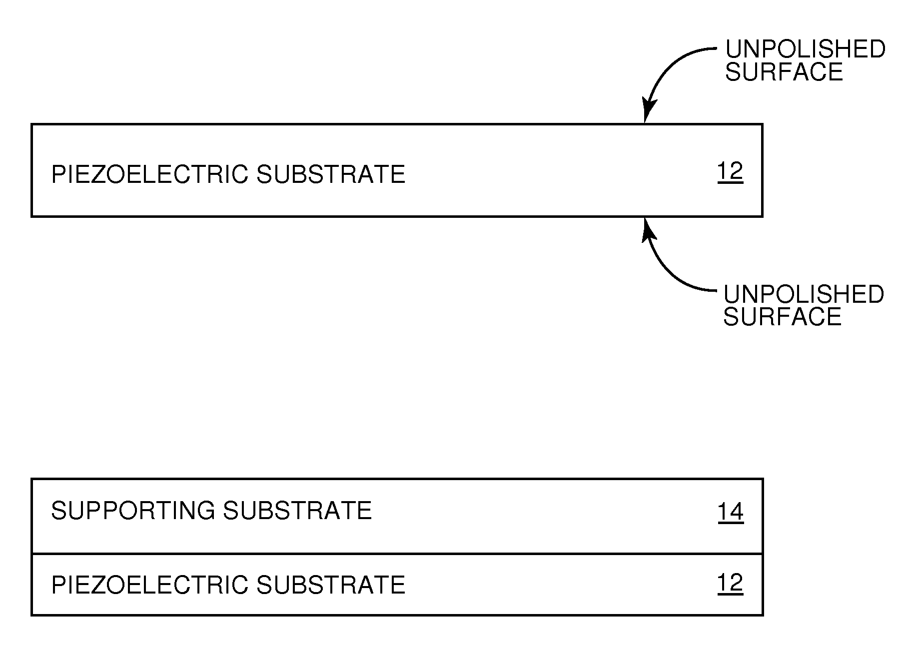
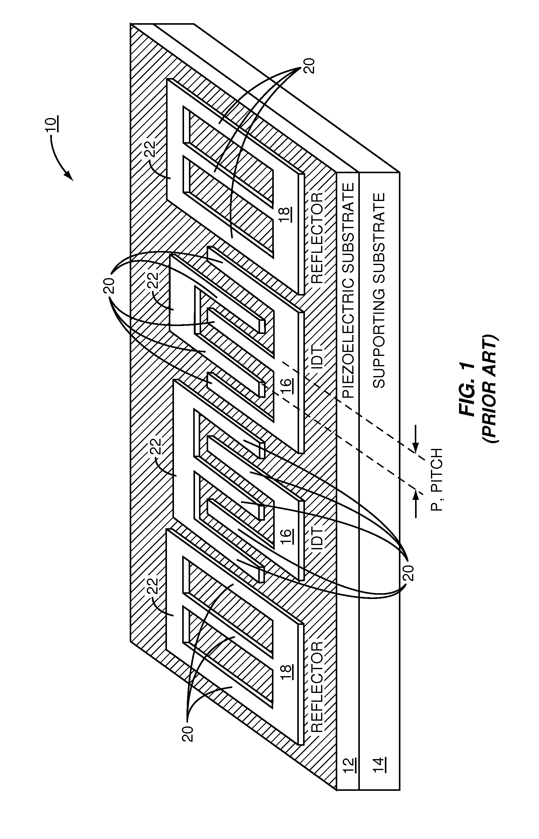
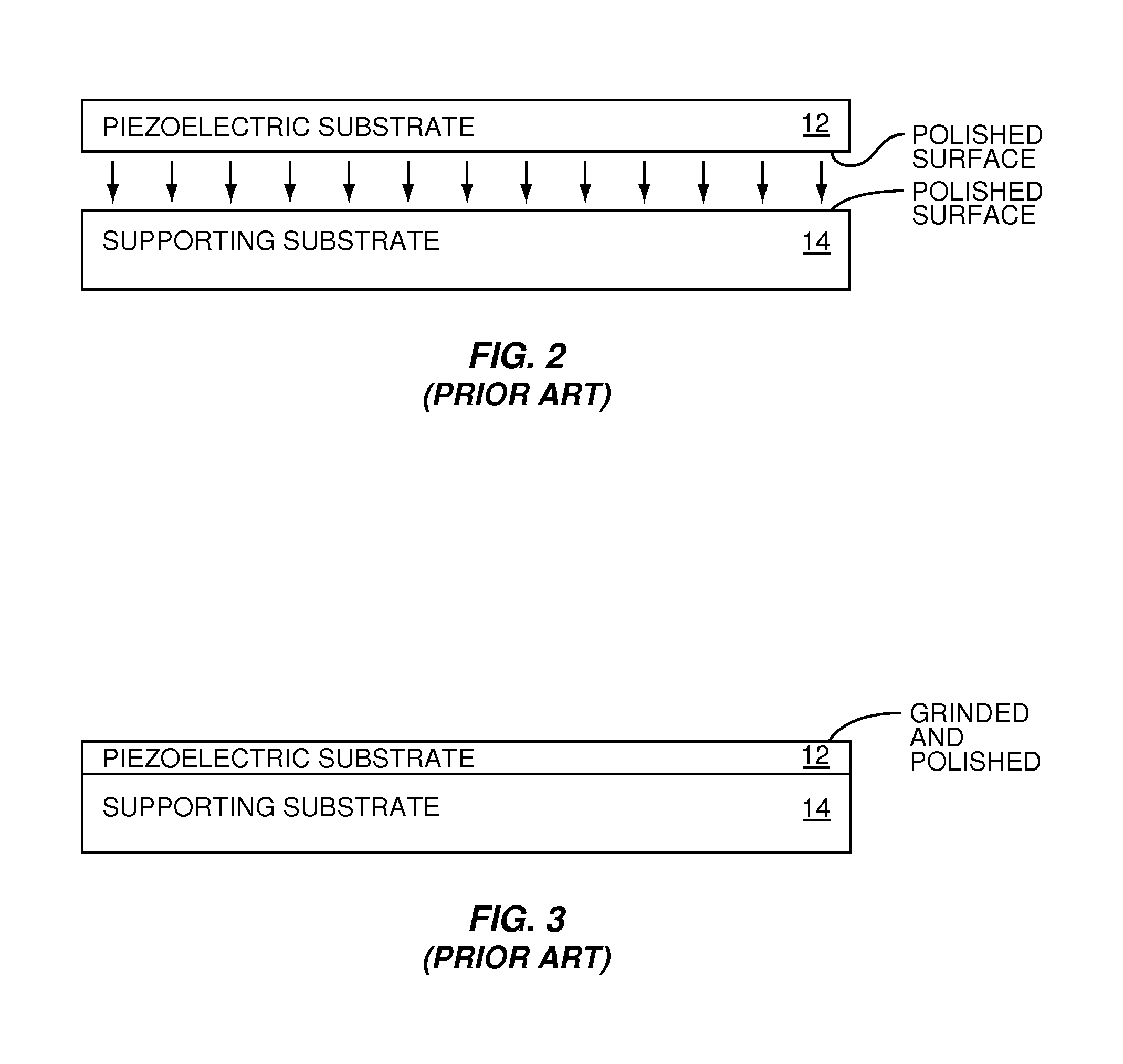
[0025]FIGS. 4 through 7 illustrate a process of manufacturing a SAW device 10 including a piezoelectric substrate 12 and a supporting substrate 14 according to the present invention. As illustrated in FIG. 4, the process begins with the piezoelectric substrate 12 having unpolished upper and lower surfaces. The piezoelectric substrate 12 has a relatively high thermal coefficient of expansion (TCE) value relative to that of the supporting substrate 14. While referred to herein as TCE, TCE may alternatively be referred to as a coefficient of thermal expansion (CTE). The isolated TCE value of the piezoelectric substrate 12 may be approximately 10 to 20 parts per million (ppm) / degree Celsius (C) and the Young's Modulus value may be approximately 30 to 500 Giga Pascals (GPa). In a preferred embodiment, the isolated TCE value for the piezoelectric substrate 12 is approximately 16 to 20 ppm / degree C. and the Young's Modulus value is approximately 200 GPa. The piezoelectric substrate 12 may ...
second embodiment
[0029]FIGS. 8 through 12 illustrate a process of manufacturing the SAW device 10 having the piezoelectric substrate 12 and the supporting substrate 14 according to the present invention. As illustrated in FIG. 8, the process begins with the piezoelectric substrate 12. One surface is polished. The other surface of the piezoelectric substrate 12 is preferably unpolished. However, the present invention is not limited thereto. The other surface of the piezoelectric substrate 12 may alternatively be polished. Then, as illustrated in FIG. 9, the polished surface of the piezoelectric substrate 12 is attached to a temporary carrier substrate 24, and the unpolished or unattached side of the piezoelectric substrate 12 is grinded or otherwise processed to thin the piezoelectric substrate 12 to a desired thickness. The piezoelectric substrate 12 may be attached to the temporary carrier substrate 24 by a glue bonding process or the like. As illustrated in FIG. 10, once the piezoelectric substrat...
PUM
| Property | Measurement | Unit |
|---|---|---|
| Fraction | aaaaa | aaaaa |
| Temperature | aaaaa | aaaaa |
| Thickness | aaaaa | aaaaa |
Abstract
Description
Claims
Application Information


