Diffraction grating, organic EL element using the same, and manufacturing methods thereof

a technology of organic el elements and gratings, applied in the direction of optical elements, instruments, other domestic objects, etc., can solve the problems of insufficient performance of organic el elements and difficult white light emission, and achieve the effect of low wavelength dependence and low directivity

Active Publication Date: 2013-09-24
JX NIPPON OIL & ENERGY CORP +1
View PDF12 Cites 15 Cited by
  • Summary
  • Abstract
  • Description
  • Claims
  • Application Information

AI Technical Summary

Benefits of technology

[0054]According to the present invention, it is possible to provide a diffraction grating having a sufficiently low wavelength-dependence and a sufficiently low directivity, an organic EL element using the diffraction grating, and methods for manufacturing the diffraction grating and the organic EL element.

Problems solved by technology

Although having been improved in terms of the problem of the external extraction efficiency, the organic EL element as described in Patent Literature 1 still has problems that white light emission is difficult because of its high wavelength-dependence of light emission, and that the directivity of light emission (a characteristic of emitting light strongly in a certain direction) is high.
Hence, the performances of the organic EL element are not necessarily sufficient.

Method used


Image

  • Diffraction grating, organic EL element using the same, and manufacturing methods thereof
  • Diffraction grating, organic EL element using the same, and manufacturing methods thereof
  • Diffraction grating, organic EL element using the same, and manufacturing methods thereof

Examples


fabrication example 1

[0319]First, a silicone-based polymer [a resin composition of a mixture of 90% by mass of a silicone rubber (manufactured by Wacker Chemie AG under the product name of “Elastosil RT601”) and 10% by mass of a curing agent] was applied onto a base member (material: glass, size: 20 mm×12 mm) by a spin coating method, and cured by being heated at 100° C. for 1 hour. Thus, a silicone-based polymer film was formed.

[0320]Next, an aluminum vapor-deposition film (thickness: 10 nm) was formed on the silicone-based polymer film by a vapor deposition method under conditions of a temperature of 100° C. and a pressure of 1×10⁻³ Pa. Then, after cooling to room temperature (25° C.) over a period of 30 minutes, the pressure was returned to the atmospheric pressure (1.013×10⁵ Pa). Consequently, concavities and convexities were formed on a surface of the aluminum vapor-deposition film formed on the silicone-based polymer film. Subsequently, a silicone-based polymer [a resin composition of a mixture of...

fabrication example 2

[0322]First, an azobenzene polymer was applied in a film thickness of 0.8 μm onto a base member (material: glass, size: 15 mm×12 mm) by a spin coating method. Thus, an azobenzene polymer film was formed. Then, argon laser light was diffracted with a surface relief-type diffraction grating, and the surface of the azobenzene polymer film was irradiated with the diffracted light. Next, the diffraction grating was rotated by 120°, then laser light was diffracted, and the azobenzene polymer film was irradiated with the diffracted light. Subsequently, the diffraction grating was further rotated by 120°, then laser light was diffracted, and the azobenzene polymer film was irradiated with the diffracted light. Thus, concavities and convexities were formed on the surface of the azobenzene polymer film in a periodic arrangement.

[0323]Next, a silicone rubber (manufactured by Wacker Chemie AG under the product name of “Elastosil RT601”) was applied onto the azobenzene polymer film by a dropping...

example 1

[0324](i) Fabrication of Diffraction Grating

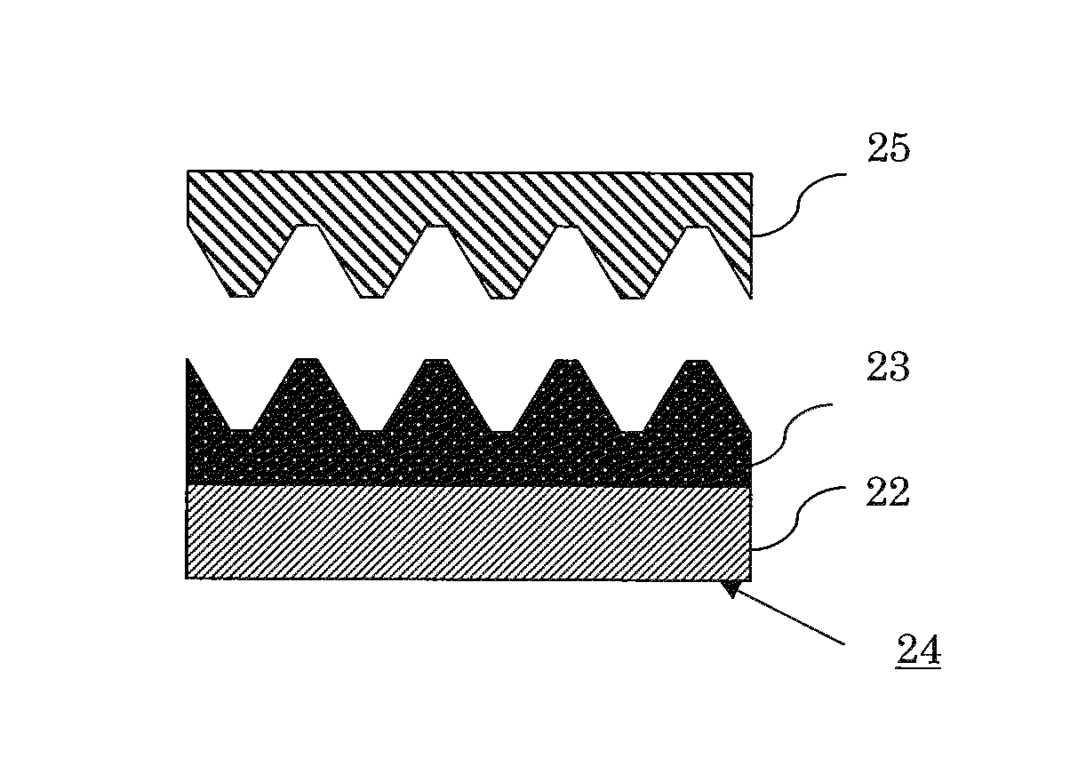
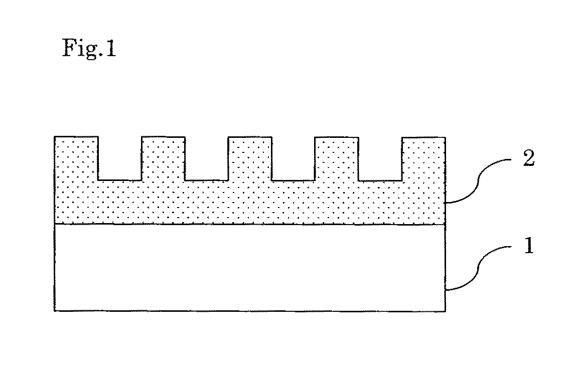
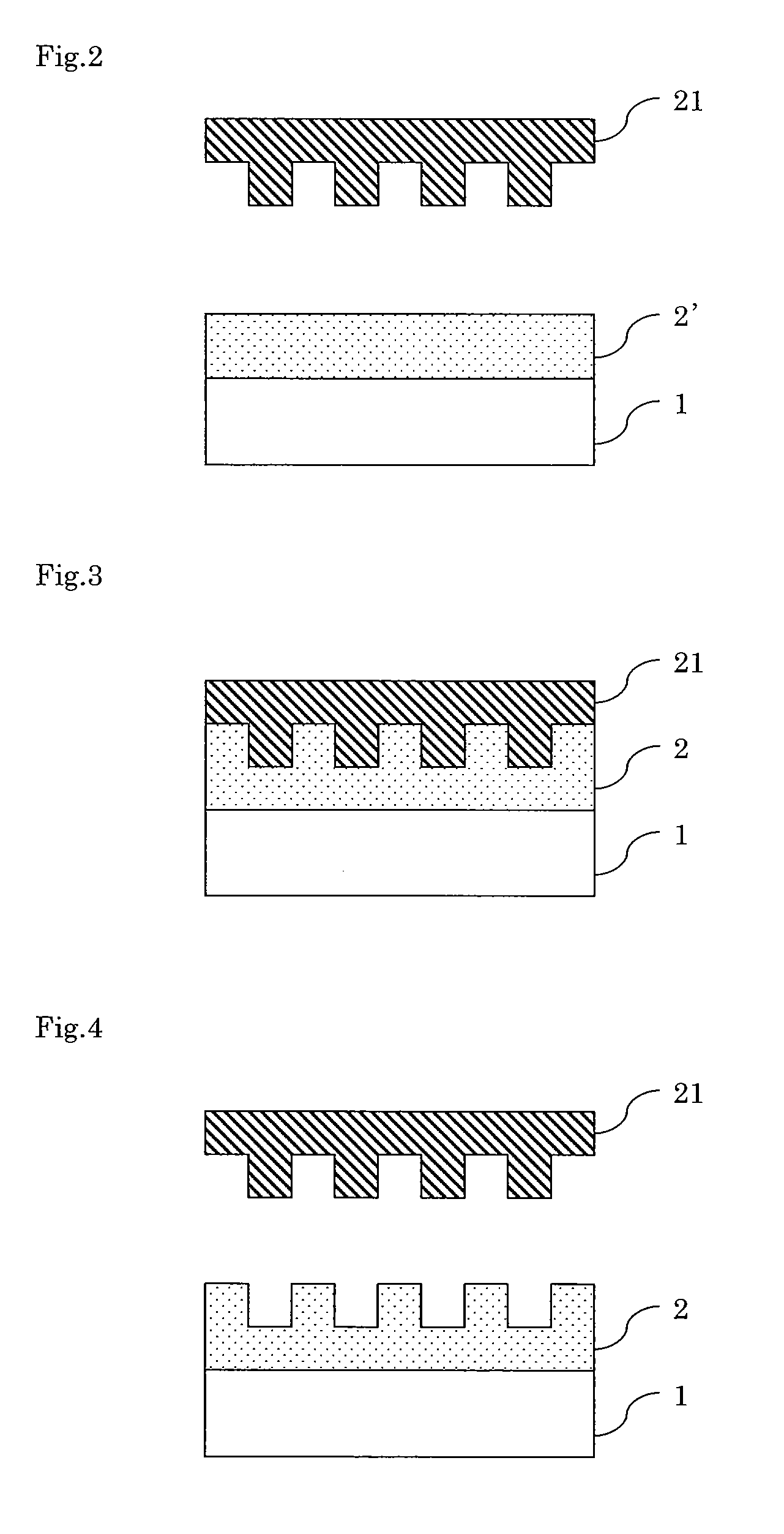
[0325]A glass substrate 1 (manufactured by Matsunami Glass Ind., Ltd. under the product name of “Micro slide glass”) and a curable resin 2′ (manufactured by Norland Optical Adhesive under the product name of “NOA 61”) were prepared. Then, the curable resin 2′ was applied onto the glass substrate 1. Thereafter, the curable resin 2′ was cured by irradiation with ultraviolet rays for 1 hour, with Master Block (M-3B) obtained in Fabrication Example 1 being pressed thereto (see FIGS. 2 and 3). Then, Master Block (M-3B) was detached from the cured resin layer 2, and thereby the cured resin layer 2 having concavities and convexities formed thereon was formed on the glass substrate 1. Thus, a diffraction grating was obtained (see FIG. 4).

[0326]A concavity and convexity analysis image was obtained by analyzing the shape of the concavities and convexities formed on the surface of the cured resin layer in the obtained diffraction grating by use of an...


PUM


Abstract

A diffraction grating having a transparent supporting substrate; and a cured resin layer which is stacked on the transparent supporting substrate and which has concavities and convexities formed on a surface thereof, wherein when a Fourier-transformed image is obtained by performing two-dimensional fast Fourier transform processing on a concavity and convexity analysis image obtained by analyzing a shape of the concavities and convexities formed on the surface of the cured resin layer by use of an atomic force microscope, the Fourier-transformed image shows a circular or annular pattern substantially centered at an origin at which an absolute value of wavenumber is 0 μm−1, and the circular or annular pattern is present within a region where an absolute value of wavenumber is within a range of 10 μm−1 or less.

Description

CROSS-REFERENCE TO RELATED APPLICATIONS[0001]This is a U.S. National Phase of International Application PCT / JP2010 / 062110, filed Jul. 16, 2010, and claims the benefit of foreign priority from Japanese Patent Application 2009-168056, filed Jul. 16, 2009; Japanese Patent Application 2009-200436, filed Aug. 31, 2009; and Japanese Patent Application 2009-297868, filed Dec. 28, 2009, the entire disclosures of which applications are hereby incorporated herein by reference.TECHNICAL FIELD[0002]The present invention relates to a diffraction grating, an organic EL element using the same, and manufacturing methods thereof.BACKGROUND ART[0003]Organic electroluminescence elements (organic EL elements) have been used as self-luminous elements for image display devices, such displays, and for surface light sources. Such an organic EL element (organic light-emitting diode (OLED)) is generally prepared by stacking a transparent electrode serving as an anode, an organic layer, and a metal electrode ...

Claims


Application Information

Patent Timeline
Patent Type & Authority Patents(United States)
IPC IPC(8): H01L51/52
CPCG02B5/1809H01L51/5275H05B33/10H01L2251/105H10K50/858H10K71/821Y10S428/917
Inventor SEKI, TAKASHINISHIMURA, SUZUSHIFUKUDA, MAKIFUKUSHIMA, MADOKAMASUYAMA, SATOSHIJEONG, SOON MOONTAKEZOE, HIDEOKOO, WON HOE
Owner JX NIPPON OIL & ENERGY CORP
Why Eureka
Try Eureka