ADC first stage combining both sample-hold and ADC first stage analog-to-digital conversion functions

a technology of analog-to-digital conversion and first stage, which is applied in the field of analog-to-digital converters (adcs), can solve the problems of small nonlinear error, increase the amount of power required by the adc, and consume a large fraction of the total adc power

Active Publication Date: 2013-12-10
LEWYN CONSULTING
View PDF6 Cites 36 Cited by
  • Summary
  • Abstract
  • Description
  • Claims
  • Application Information

AI Technical Summary

Problems solved by technology

However, the most common pipeline ADCs must be preceded by a sample-and-hold-plus-amplifier (SHA) stage which significantly increases the amount of power required by the ADC.
One unfortunate characteristic of a high-speed TH or SHA input stage is that in order to not substantially degrade the signal-to-noise dynamic range (SNDR) characteristics of the subsequent pipeline stage, it must consume a high fraction of the total ADC power.
Any failure to achieve complete voltage settling results in a small nonlinear error.
Hence, the solution to the separating the CS and CDAC capacitors is not a viable low-power solution for high sample rate ADC applications.
As is well understood by persons of ordinary skill in the design of operational amplifiers, if the ADC capacitive load on the BAMP is removed for a period of time, such as half an ADC sample clock period, the removal and consequently reduced capacitive load could lead to an instability which could cause either the output of an operational transconductance, or current-output BAMP (OTA) to begin uncontrolled oscillation for a brief period of time.
Non-linear capacitances are well known contributors to high frequency amplifier distortion.
The Devarajan reference does describe how the time delay from sampling the final value of the input signal to the time that the comparators produce a reliable output adversely affects how the time available for the MDAC RAMP to fully settle is shortened.
This adverse effect of the comparator time delay is to shorten the HOLD time interval.
The Devarajan reference qualitatively describes how the additional comparator power required to shorten the comparator delay time required to accommodate increasing ADC clock rates (shorter ADC clock periods) results in a significant sampling frequency limitation in SHA-less ADCs.
The major contributor to such error rates is the susceptibility of the comparator to what is commonly known as comparator metastability errors.
This requirement arises from the fact that although the SADC sample occurs at the same time as the input signal is sampled across CS, differences in the SADC input time response and the time response of the BAMP charging CS can result in SADC quantization error consuming an unacceptably large fraction of the MDAC error correction range.
The SADC-BAMP Bandwidth Matching Limitation becomes a severe limitation when the input signals have significant frequency components near the maximum bandwidth of the IC components used in the SADC-BAMP.
For example, this matching limitation becomes severe when input signal bandwidths exceed 1 GHz and also in cases where multiple pipeline ADCs of lower bandwidth are interleaved to quantize higher bandwidth input signals.
It avoids the technique of auto-zeroing the amplifier to reduce 1 / f noise because “auto-zeroing the amplifier can help reduce 1 / f noise at the expense of increased complexity and power.” Unfortunately, most other methods are not nearly as effective as auto-zeroing for reducing 1 / f noise.
The limitation of operating the RAMP with only common-mode DC offset correction, will be hereinafter referred to as the Amplifier Common-Mode Offset Correction Limitation, because this common-mode offset correction does not correct for input DC offsets.
However, the prior art of U.S. Pat. No. 7,450,050, Nov. 11, 2008, by A. Rezayee, et. al. employed small autozeroing capacitors (CRESET_1224-1 and CRESET_2224-2 in FIG. 2b) and switches in an arrangement which add little complexity to the stage and, as stated in the patent, also consume little additional power.
While not greatly amplifying the input DC offset, unfortunately the amplifier input DC offset will still be present in the RAMP output after reset.
The accumulation of DC offset in a sequence of pipeline ADC stages is detrimental to the overall ADC performance because it subtracts from the available voltage headroom which, in turn, limits output signal swing.

Method used


Image

  • ADC first stage combining both sample-hold and ADC first stage analog-to-digital conversion functions
  • ADC first stage combining both sample-hold and ADC first stage analog-to-digital conversion functions
  • ADC first stage combining both sample-hold and ADC first stage analog-to-digital conversion functions

Examples


Embodiment Construction

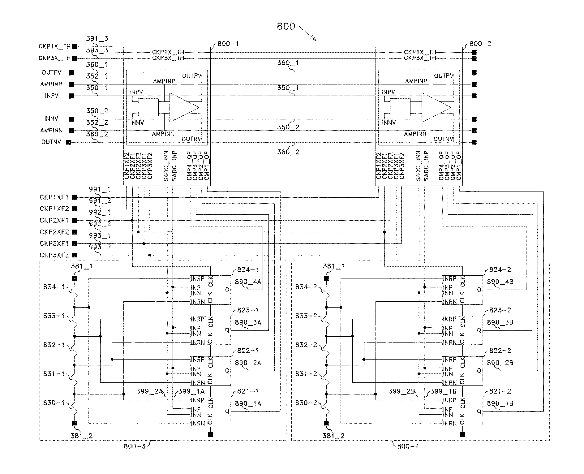
[0041]Various aspects of embodiments, some or all of which may be included in different implementations of the invention, offer corresponding advantages relative to the prior art. For example, one aspect addresses the limitations present in the Devarajan and Rezayee systems to achieve SHA-less pipeline ADC sampling rates up to, and beyond, the GSPS region of operation by combining the track and hold functions of an SHA-less pipeline ADC with the first stage MDAC functions of a pipeline ADC. These limitations may be overcome by duplicating the resulting ADC first stage circuit to create a first ADC first stage and a second ADC first stage, connecting the analog inputs of the first and second ADC first stages, and providing a novel combination of CMOS capacitors, residue amplifiers, switches, autozero circuits, and different timing intervals to reduce 1 / f noise contribution, DC offset, and set the residue amplifier common-mode output voltage. Such different timing intervals are facili...


PUM


Abstract

A first stage circuit for a pipeline ADC first stage combines the functions of an input sample-and-hold-plus-amplifier (SHA) stage, and the functions of the first analog-to-digital conversion stage of an ADC, including a multiplying DAC (MDAC), stage-flash ADC (SFADC) comparators, and residue opamp (RAMP). The ADC first stage is duplicated, inputs and outputs are connected, and an autozero circuit using a switched-capacitor filter feedback loop controls the RAMP bias circuitry to reduce 1 / f noise and DC offsets. The sampling capacitors may be connected to the ADC input for one full sample clock time period and are disconnected from the analog input period before connecting the sampling capacitors to an amplifier voltage output or voltage reference, thereby sampling the input and allowing sufficient time for the SFADC comparators to resolve and control the MDAC capacitor settings with a low metastability error rate.

Description

TECHNICAL FIELD[0001]This invention pertains to analog-to-digital converters (ADCs), and particularly to ADCs for telecommunication applications fabricated using integrated circuit (IC) technology.BACKGROUND OF THE INVENTION[0002]The integrated circuit (IC) electronics industry is currently expending significant amounts of research money on improving the performance of ADCs telecommunication applications. Applications ranging from mobile communications to copper and fiber networks are requiring higher speeds and lower power. Pipeline ADC architectures are the most commonly chosen for these applications as they provide a good combination of high speed and low power. However, the most common pipeline ADCs must be preceded by a sample-and-hold-plus-amplifier (SHA) stage which significantly increases the amount of power required by the ADC. Extensive research efforts in IC pipeline ADC technology have been directed toward the goal of modifying the first pipeline stage so that it can als...

Claims


Application Information

Patent Timeline
Patent Type & Authority Patents(United States)
IPC IPC(8): H03M1/34
CPCH03M1/0863H03M1/167H03M1/44
Inventor LEWYN, LANNY L
Owner LEWYN CONSULTING
Why Eureka
Try Eureka