Device and method for generating clock signals for DC-DC converters

a clock signal and converter technology, applied in the direction of automatic control, process and machine control, instruments, etc., can solve the problems of reducing the size of the required electronic circuit and the manufacturing cost of the electronic device, so as to achieve the effect of not occupying additional space on the circuit and without extra cos

Active Publication Date: 2013-12-31
TEXAS INSTR INC
View PDF10 Cites 2 Cited by
  • Summary
  • Abstract
  • Description
  • Claims
  • Application Information

AI Technical Summary

Benefits of technology

[0006]It is an object of the invention to provide an electronic device and a method for DC-DC conversion having reduced EMI emission without a need of external components or much additional silicon area.
[0008]An electronic device that is configured in accordance with advantageous aspects of the invention includes a DC-DC converter that is configured to be used in slave and master mode. The electronic device includes a phase locked loop (PLL). When the electronic device is configured in slave mode (first configuration), the PLL is enabled to synchronize the internal DC-DC converter clock to an external reference clock. When the electronic device is configured in master mode (second configuration), the phase locked loop can be disabled or can be adapted to generate a modulation signal for performing a spread spectrum modulation of the DC-DC converter internal clock. This internal clock, that is accessible at an output pin (often referred to as “switch pin”) of the DC-DC converter (or electronic device), can be used as master clock (or reference clock) to synchronize additional switch converters present in the system and configured as slaves. The phase locked loop may include a controlled oscillator (e.g. a voltage controlled oscillator), a filter having an integration capacitor coupled to the control input of the controlled oscillator, a charge pump, and a phase frequency detector. The output of the controlled oscillator may be the internal clock of the DC-DC converter. The controlled oscillator, the filter, the charge pump and the phase frequency detector may be coupled in a first configuration in the slave mode to operate as a normal phase locked loop for synchronizing the internal DC-DC converter clock to an external reference clock (or master clock). Furthermore, there may be a comparator which monitors the control voltage of the oscillator when the electronic device is configured as master in the master mode of the electronic device. The phase frequency detector may then be configured to be switched off. Instead of the phase frequency detector, the comparator may then be used to control the charge pump to perform a modulation of the control signal of the controlled oscillator by charging and discharging an integration capacitor of the loop filter. In that way, the low frequency signal required for the modulation of the internal DC-DC clock is obtained. Accordingly, most of the components of the phase locked loop (charge pump, integration capacitor and voltage controlled oscillator) together with the comparator may be used in the master configuration (or second configuration) to modulate the internal clock of the DC-DC converter. This provides the advantage that only very few additional components, circuitry and modifications are required to change a conventional phase locked loop into a control loop which is capable of performing an SSC modulation of the DC-DC converter clock. This reduces the size of the required electronic circuit and thereby manufacturing costs of the electronic device. This kind of implementation of the SSC modulation is possible due to the relaxed jitter requirements in switch converter (DC-DC converters) applications with respect to the much higher jitter requirements of communications and microprocessor systems.
[0009]In a preferred embodiment, the control signal at the input of the controlled oscillator may have a triangular waveform. The amplitude and frequency of the triangular waveform defines the modulation parameters (modulation ratio, modulation frequency and modulation index). The triangular waveform may advantageously be obtained by integration of a charge pump current on the integration capacitor of the loop filter. A triangular waveform is advantageous, since it easy to achieve and gives a flat distribution of the harmonics resulting from the modulation.
[0012]The controlled oscillator (or voltage controlled oscillator) may be a modified RC oscillator. It may comprise an oscillation capacitor Cosc, an oscillation resistor Rosc and a comparator. The capacitor Cosc is charged to a voltage VREFOSC at a rate defined by Rosc and Cosc (i.e. by the Rosc x Cosc time constant). The comparator monitors the capacitor voltage and discharges it when VREFOSC has been reached. This is an advantageous way to generate a clock (comparator output) and at the same time a ramp or sawtooth waveform (capacitor voltage) required for DC-DC converters using pulse width modulation. The optimum method of modulating the clock frequency in order to perform the spread spectrum clocking (SSC) is varying slightly the slope of the generated ramp. In order to vary the ramp slope, a controlled current source may be implemented in the electronic device and configured to supply a current to the oscillation capacitor which is proportional to the control signal.
[0013]The invention also provides a system including at least two electronic devices configured in accordance with aspects of the invention, i.e., for example a first DC-DC converter and a second DC-DC converter. One DC-DC converter may be configured to operate in master mode and one or more other DC-DC converters may be configured to operate in slave mode. The DC-DC converters running in slave mode may be synchronized to the master clock (modulated clock signal) from the DC-DC converter running in master mode. Using spread spectrum clocking and synchronization together prevents generation of intermodulation bands that can fall into audio frequencies and cause interference. As set out above, the modulation stage may be implemented by the first control loop. In other words, the first control loop in the master DC-DC converter performs the spread spectrum modulation of the frequency of the first clock signal and the slave devices synchronize to the first clock frequency. This means that only few additional components are required to implement the modulation stage in the master device, which simplifies production and reduces chip area. The bandwidth of the phase locked loops of the DC-DC converters used in slave mode should be wide enough in order to be able to track the spread spectrum clocking modulation from the master DC-DC converter. The PLL function of the master DC-DC converter can be disabled and most of the PLL blocks can be reused to perform an SSC modulation of the switching frequency. Then, the SSC function can be enabled only for the DC-DC converter which is the master device and the synchronization function can be enabled only for the DC-DC converter or DC-DC converters which are in slave mode. Therefore, no significant additional silicon area is required to obtain the spread spectrum clocking function.
[0015]The invention also provides a method of synchronizing a first clock signal having a first clock frequency controlled by a first control loop and a second clock signal having a second clock frequency controlled by a second control loop. The first and second clock signals may be configured to be used for voltage conversion. Furthermore, a control signal is generated to perform a spread spectrum modulation of the first clock frequency, and the second clock signal is synchronized with the spread spectrum modulated first clock signal. Performing both a synchronization of the first clock signal and the second clock signal and a spread spectrum clocking of the first clock signal allows intermodulation products in sensitive frequency bands such as the audio band to be reduced, which would otherwise cause interference with required signals. Using just a part of the first phase locked loop, for example, and switching off the functionality of the phase frequency detector means that no extra circuitry is required in the DC-DC converter. Therefore, existing designs can be simply adapted to perform the method of the present invention without extra cost and without taking up additional space on the circuit.

Problems solved by technology

This reduces the size of the required electronic circuit and thereby manufacturing costs of the electronic device.

Method used


Image

  • Device and method for generating clock signals for DC-DC converters
  • Device and method for generating clock signals for DC-DC converters
  • Device and method for generating clock signals for DC-DC converters

Examples


Embodiment Construction

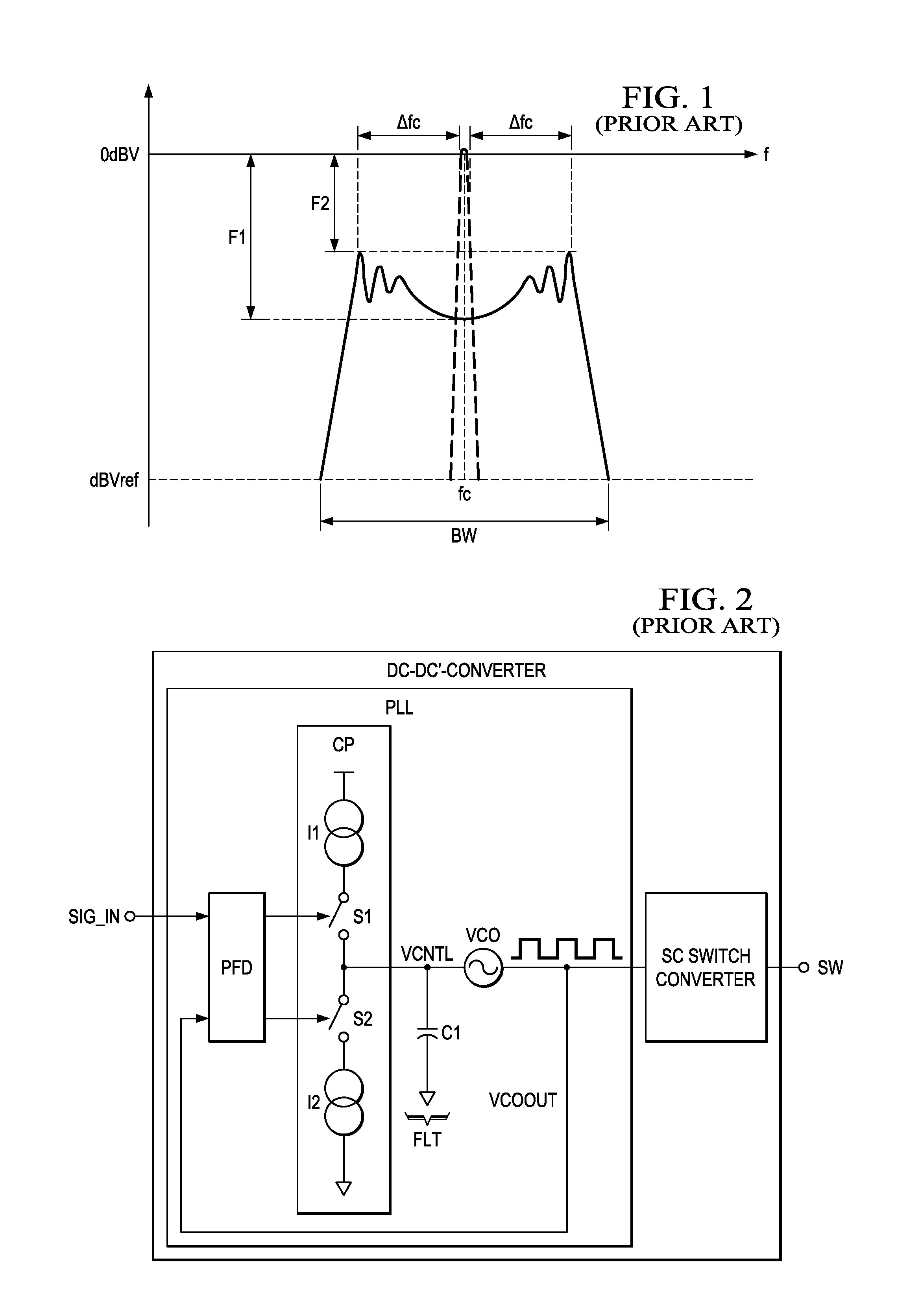
[0023]FIG. 1 is a graphical representation based on a publication of Santolaria et al., EMI Reduction in Switched Power Converters by means of Spread Spectrum Modulation Techniques, 35th Annual IEEE Power Electronics Specialists Conference, pp. 292-296, Aachen, Germany. FIG. 1 shows the amplitude as a function of frequency of spread spectrum modulation of a signal having a carrier frequency fc. A non-modulated harmonic of the carrier frequency, centered about the carrier frequency fc, is shown as a dotted line, with a modulated signal, also centered about the carrier frequency fc and having side band harmonics, being shown as a solid line. The modulated signal has a bandwidth BW.

[0024]The modulation index mf is defined as

[0025]mf=δ·fcfm,

[0026]where fc is the carrier frequency, fm is the modulation frequency and δ is the modulation ratio. δ is defined as

[0027]δ=Δ⁢⁢fcfc.

[0028]Δfc is the peak deviation of the carrier frequency. The carrier frequency fc is modulated by the modulation fr...


PUM


Abstract

An electronic device includes a DC-DC converter for voltage conversion in a slave mode an in a master mode and including a phase locked loop. The phase locked loop comprises a controlled oscillator, a filter having an integration capacitor coupled to a control input of the controlled oscillator, a charge pump, and a phase frequency detector. In the slave mode, the controlled oscillator, the filter, the charge pump and the phase frequency detector are coupled to operate as the phase locked loop. There is a comparator coupled with an input to a control input of the controlled oscillator and with an output to the charge pump. In the master mode, the comparator is configured to control the charge pump in response to a control signal at the control input of the controlled oscillator when the phase frequency detector is switched off so as to perform a modulation of the control signal at the control input of the controlled oscillator by charging and discharging the integration capacitor.

Description

CROSS-RELATED APPLICATIONS[0001]This patent application claims priority from German Patent Application No. 10 2008 053 670.9, filed Oct. 29, 2008 and from U.S. Provisional Patent Application No. 61 / 141,817, filed Dec. 31, 2008, the entirety which are incorporated herein by reference.FIELD OF THE INVENTION[0002]The present invention generally relates to a device and method for generating clock signals for DC-DC converters.BACKGROUND OF THE INVENTION[0003]Switching frequency in power converters (for example DC-DC buck and boost converters) is limited mainly by the ability of power transistors to manage large power with short switching times. As new process generations improve the switching quality factor, higher switching frequencies in DC-DC converters can be achieved in order to reduce the size of the passive components and increase the power efficiency. A drawback of achieving higher switching frequencies is that, as the operating frequency is increased, the current and voltage pre...

Claims


Application Information

Patent Timeline
Patent Type & Authority Patents(United States)
IPC IPC(8): H02M3/156H03L7/06G05F1/00
CPCH02M3/1584H02M1/44
Inventor PRIEGO, ANTONIO
Owner TEXAS INSTR INC
Why Eureka
Try Eureka