
Signal level shift circuit and method for dual resistor ladder digital-to-analog converters

a dual resistor ladder and shift circuit technology, applied in digital-analog converters, transmission systems, instruments, etc., can solve the problems of slow dac operation, increase the cost of silicon area, and reduce the resolution of the signal level shift circuit, so as to improve the resolution and accuracy of the dac, improve the signal level bit-shifting circuitry and operation.

Active Publication Date: 2013-12-31
TEXAS INSTR INC
View PDF6 Cites 23 Cited by
  • Summary
  • Abstract
  • Description
  • Claims
  • Application Information

AI Technical Summary

Benefits of technology

The invention provides a dual resistor ladder DAC and method that improve signal level bit-shifting circuitry and operation to achieve improved resolution and accuracy of the DAC without increasing the number of resistors or output impedance. The method includes coupling MOS programmable bit-shifting transistors to the coarse and fine ladders of the DAC to provide a plurality of bits of increased resolution. The transistors are turned on or off in response to bit-switching bits to provide the increased resolution. The invention improves the matching of resistive elements within the DAC over a range of fabrication processes and temperatures. The technical effects of the invention include improved signal-to-analog conversion accuracy and higher resolution of the DAC.

Problems solved by technology

Doubling the number of resistors doubles the impedance and also the parasitic capacitance of the ladders in the DAC, and consequently degrades its operating speed and increases its silicon area cost.
That causes the RC time constant at the DAC output 3 to be much longer, resulting in slower DAC operation.
However, the bit level shifting circuitry in FIG. 2A has drawbacks.
A major drawback is that the on-state switch resistance RDS(ON) of switches 24 and 25 has an impact on the DNL and INL performance of DAC 10-2.
The inadequate matching results in substantial degradation of DNL and INL performance of prior art DAC 10-2.
Unfortunately, such W / L scaling does not provide adequate matching.
Unfortunately, a large switch occupies more integrated circuit chip area and causes greater charge injection.
This may result in large voltage glitches in the DAC circuit and longer settling times during circuit operation.
Therefore, large size MOS switch transistors are required to achieve good DNL in DAC 10-2 of FIG. 2A, but unfortunately this causes higher amounts of charge injection and consequently larger voltage glitches at the DAC output 3.
A drawback of DAC 700 in FIG. 2C is that it only provides 1-bit level shifting.

Method used


Image

  • Signal level shift circuit and method for dual resistor ladder digital-to-analog converters
  • Signal level shift circuit and method for dual resistor ladder digital-to-analog converters
  • Signal level shift circuit and method for dual resistor ladder digital-to-analog converters

Examples


Embodiment Construction

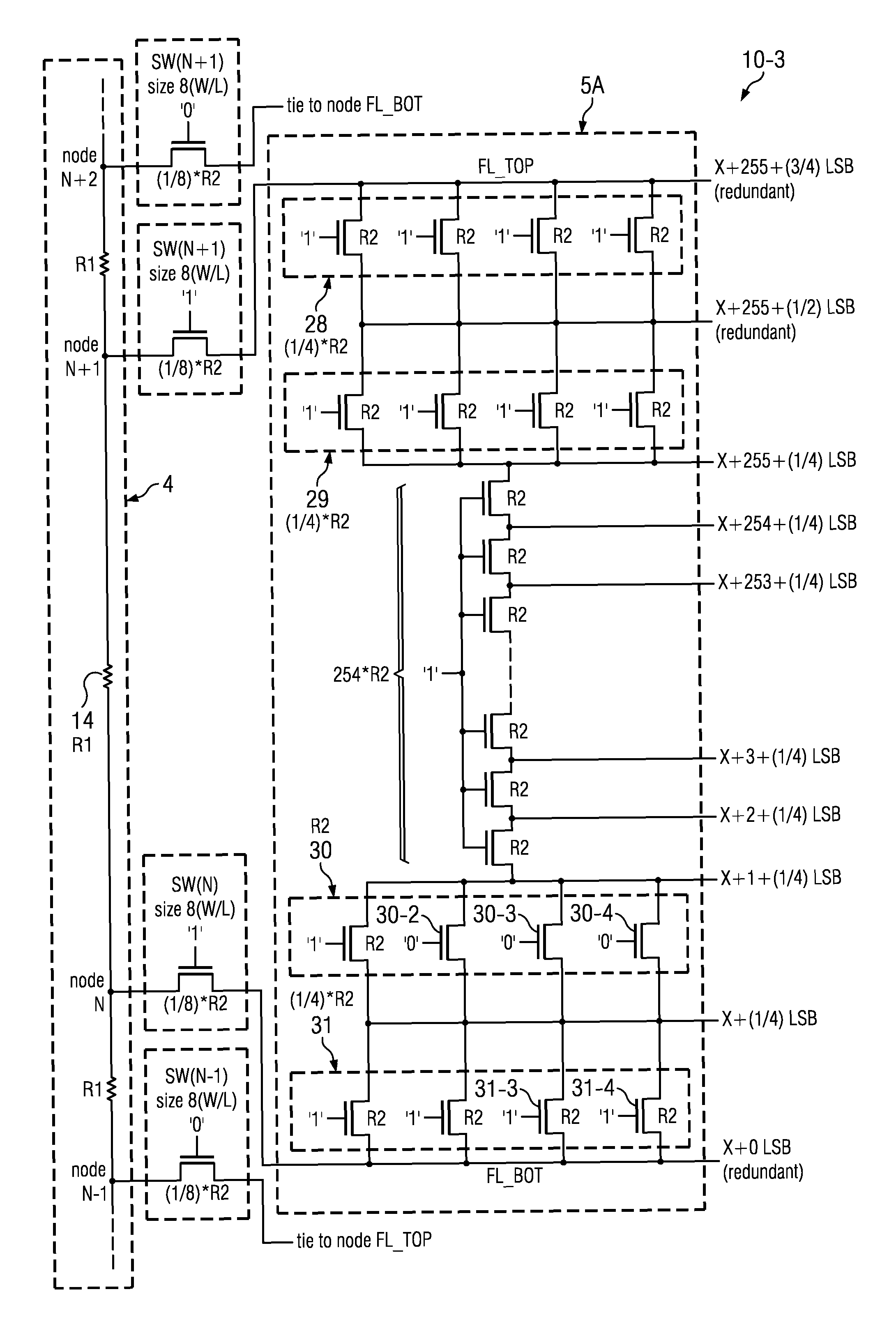
[0056]A dual resistor ladder DAC includes signal level bit-shifting circuitry and uses a corresponding signal level bit-shifting method to improve DAC resolution and accuracy without increasing the fine ladder output impedance and output capacitance and without decreasing the speed of the DAC. FIGS. 3 to 7 display a 2-bit signal level shifting scheme in the fine ladder of a dual resistor ladder DAC. The signal level bit-shifting circuitry in these drawings greatly improves the accuracy of matching between the channel resistances of various MOS transistor switches that perform fine ladder switching, the resistances of switches that perform signal level bit-shifting operations, and the “unit resistances” of poly resistors in the fine ladder. The improved matching greatly improves the DNL and INL performance of the DAC over a range of wafer fabrication process and temperature variations.

[0057]FIG. 3 consists of FIGS. 3-1 and 3-2, and illustrates the architecture of a dual resistor ladd...


PUM


Abstract

A dual resistor ladder DAC includes a coarse ladder including a plurality of coarse ladder resistors and a fine ladder including a plurality of MOS transistors coupled between first and second conductors. A first group of parallel-connected bit-shifting transistors is coupled between the first and third conductors. A second group of parallel-connected MOS bit-shifting transistors is coupled between the third and top conductors. A third group of parallel-connected bit-shifting transistors is coupled between bottom and fourth conductors. A fourth group of parallel-connected bit-shifting transistors is coupled between the second and fourth conductors. Parallel-connected bit-shifting transistors are turned either on or off in response to a plurality of bit-switching bits of a binary number to be converted. One of the bottom, first, second, third, and top conductors is coupled to a DAC output conductor in response to the plurality of bit-switching bits.

Description

BACKGROUND OF THE INVENTION[0001]The present invention relates generally to increasing the resolution of a digital-to-analog converter (DAC) having a predetermined number of bits, and more particularly, to signal level shift shifting circuitry and corresponding methodology in a dual resistor ladder DAC.[0002]Important considerations in designing a DAC usually include determining and obtaining both a required amount of resolution, which relates to differential nonlinearity (DNL), and required amount of accuracy, which relates to integral nonlinearity (INL). Other important considerations include the required operating speed, component count, integrated circuit chip area, current consumption, and power dissipation of the DAC. An appropriate DAC architecture may be chosen from various options depending on application requirements and specifications. A dual resistor ladder architecture is usually chosen for some applications, for example in a voice coil motor position control loop of a ...

Claims


Application Information

Patent Timeline
IPC IPC(8): H03M1/66
CPCH03M1/68H03M1/66
Inventor LI, QUNYING
Owner TEXAS INSTR INC
Learn More