Electrode patterning

a technology of electromechanical patterning and electrodes, which is applied in the manufacture of electromechanical systems, cold cathode manufacturing, electric discharge tubes/lamps, etc., can solve the problems of low aperture ratio, limited display area, and reduced aperture ratio, so as to avoid degradation of the underlying structure and reduce laser energy

Inactive Publication Date: 2014-04-01
FLEXENABLE LTD
View PDF10 Cites 0 Cited by
  • Summary
  • Abstract
  • Description
  • Claims
  • Application Information

AI Technical Summary

Benefits of technology

[0015]The present invention aims to provide an improved method for defining organic pixel electrodes on multi-level structures using a laser ablation type process. Embodiments have been shown to leave the underlying layers substantially unharmed and produce substantially no excess debris.

Problems solved by technology

One problem that is shared between conventional thin film transistor (TFT) technology and organic semiconductor-based printed TFTs alike is the limited display area, in which the thin film transistor, the gate line, the pixel capacitor and the pixel itself compete with each other for space.
This can lead to a reduction in the aperture ratio and therefore the quality of the display.
In conventional display architectures, printed electrodes and printed pixel capacitors tend to be large and result in active matrix displays with low aperture ratios.
However, these are relatively low resolution techniques that rely heavily on the wetting properties of the printing surface.
However, this process uses a transfer layer that would need to disposed of after it is used, and it is unlikely that laser transferred conductive material would fill the via hole which would be required for it to act as a pixel electrode.
This teaches the use of ultraviolet laser radiation, which is absorbed by most polymer layers and could cause detrimental effects to the performance of the TFT's.
This is particularly problematic with many organic semiconductor devices.
Using ultraviolet radiation as described in the prior art for top level patterning for multilayer polymer stacks will tend to cause damage of underlying layers.
In addition, such ultraviolet radiation patterning has been shown to produce debris.
The formation of debris can cause poor contact with the display medium and may lead to shorts between conductive pads.

Method used


Image

  • Electrode patterning
  • Electrode patterning
  • Electrode patterning

Examples


example 1

Direct-Write Patterning of Top Conductive Electrode

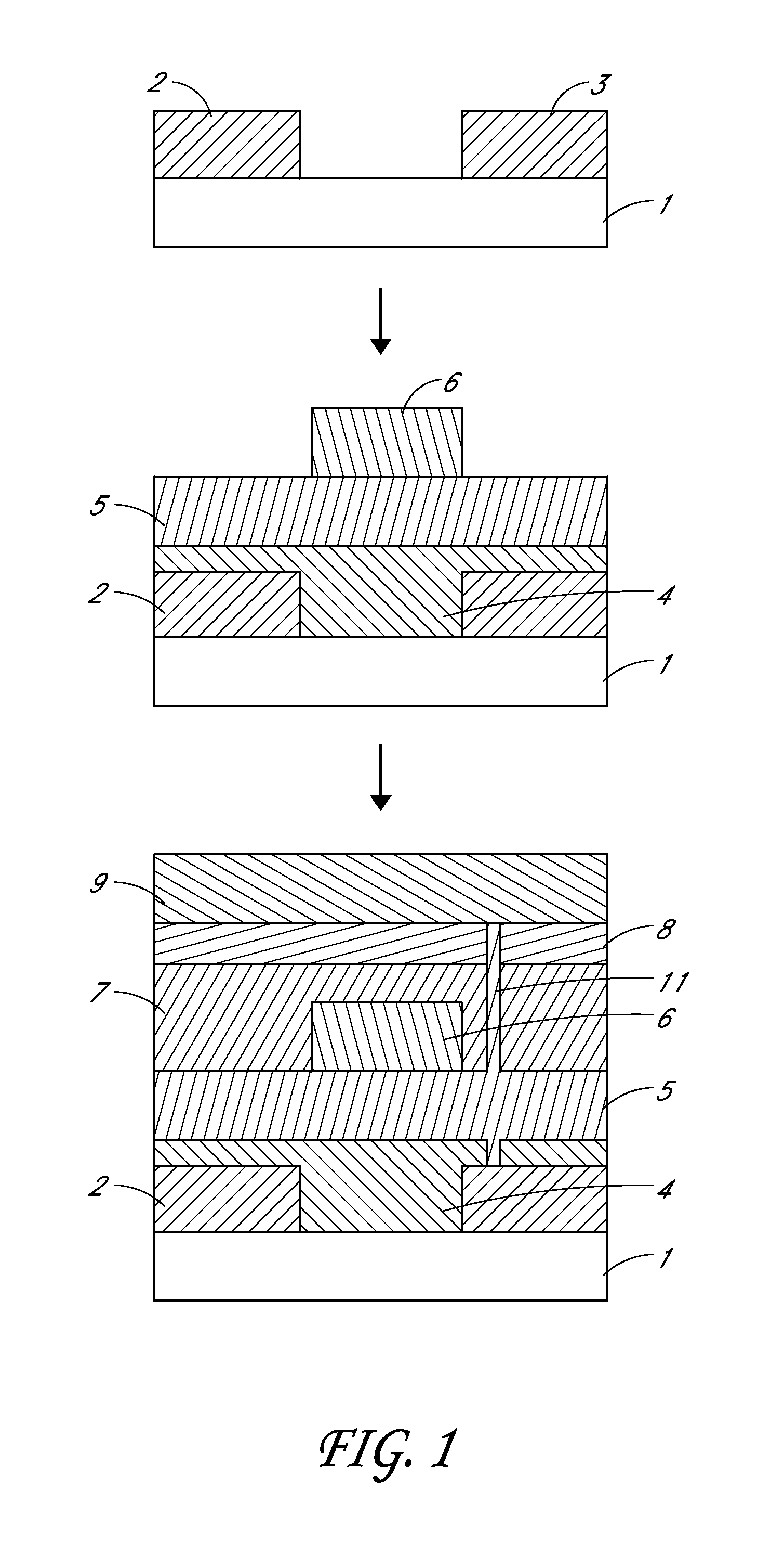
[0049]The fabrication of a multi-level (or -layer) stack for polymer-based printed TFTs according to a conventional method is illustrated in FIG. 1. Conductive material is deposited and patterned on a substrate 1 to form source and drain electrodes 2. The substrate may be either glass or a polymer film, but preferably a plastic substrate such as polyethyleneterephtalate (PET) or polyethylenenaphtalene (PEN) is used. The patterned conductive layer 2 comprises a conducting polymer, such as PEDOT, or a metallic material, such as gold or silver. It may be deposited and patterned through solution processing techniques such as, but not limited to, spin, dip, blade, bar, slot-die, or spray coating, inkjet, gravure, offset or screen printing, or evaporation, and photolithography techniques.

[0050]Once the conductive layer has been patterned to form the source and drain electrodes, a layer of semiconducting material 4 may then be deposited ov...

example 2

Patterning of the Top Conductive Layer Using a Light Absorbing Layer

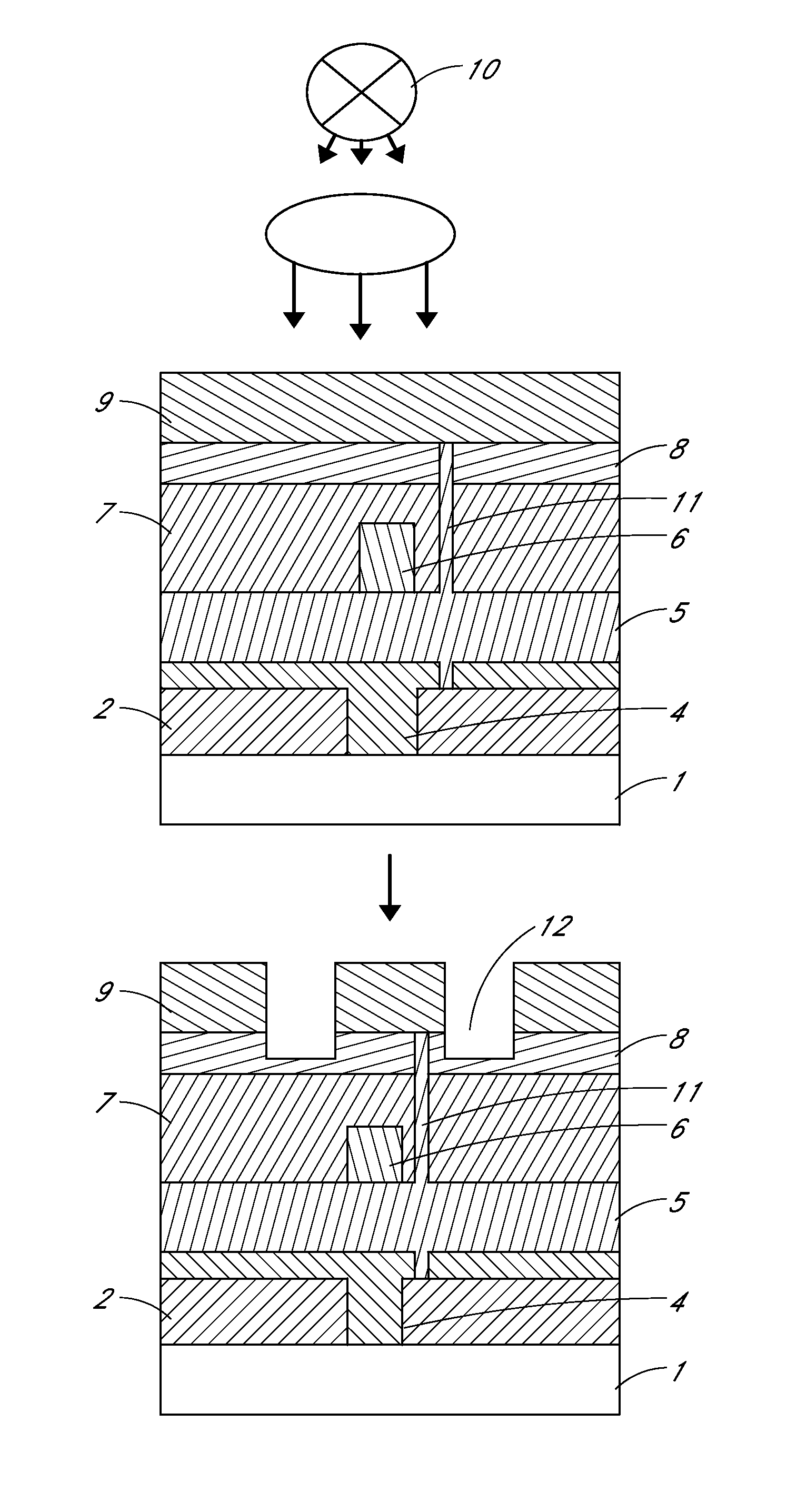
[0057]FIG. 2 illustrates a first embodiment of the present invention. In this and later examples like elements to those of FIG. 1 are indicated by like reference numerals. The top conductive layer for the pixel electrode is defined by the division of conductive layer to produce separate electrode pads on a polymer surface, and therefore creating devices with mutually isolated pixel electrode lines. An insulating wetting layer 8, which contains a dye, that absorbs IR radiation, is deposited on top of the second dielectric 7. The material of the insulating layer may be deposited from solution in the form of a continuous layer using techniques such as, but not limited to, spincoating, ink-jet printing, spray-coating, roller coating spray or blade coating. However, preferably, the technique of spray coating is used. As stated above for the dielectric layers, this insulating layer is deposited in such a way so as to inhi...

example 3

Patterning of Top Conductive Layer by Using an Optically Thick Dielectric Layer and Infrared Light

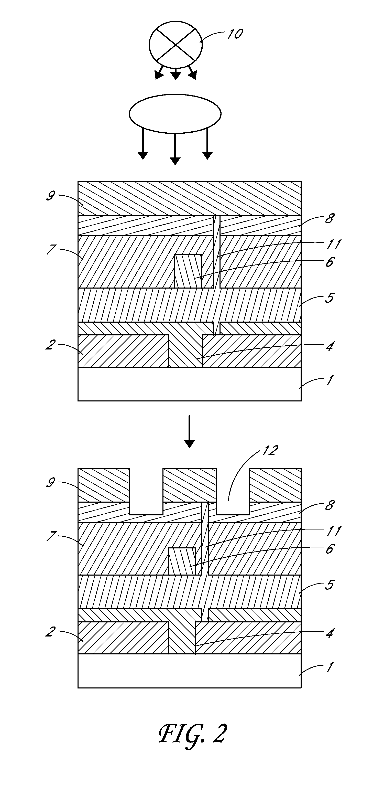
[0066]FIG. 6 illustrates a variant of a process based on the first embodiment wherein the IR absorbing moiety is added to a thick dielectric material. The second dielectric layer 7, which has an added moiety which absorbs IR radiation, is deposited on top of gate interconnect 6. The material of the second dielectric layer may be deposited from solution in the form of a continuous layer using techniques such as, but not limited to, spincoating, inkjet printing, spray-coating, roller coating spray or blade coating. However, preferably, the technique of spray coating is used. The dielectric material may also be deposited using vapour phase deposition techniques like evaporation or chemical vapour deposition. As is described above for the first embodiment, and is referred to in WO01 / 47043, the material of the dielectric layer is preferably deposited in such a way so as to inhibit degradatio...


PUM

PropertyMeasurementUnit
thicknessaaaaaaaaaa
thicknessaaaaaaaaaa
optical densityaaaaaaaaaa

Abstract

A method is provided to isolated conductive pads on top of a multi-layer polymer device structure. The method utilizes laser radiation to ablate conductive material and create a non-conductive path, electrically isolating the conductive pads. The process is self-limiting and incorporates at least one layer within the stack that absorbs the radiation at the required wavelength. The prevention of radiation degradation of the underlying layers is achieved, as absorption of radiation occurs primarily on the surface of the structure, but not in any of the radiation sensitive underlying layers of the electronic device. The method preferably uses low energy infrared radiation which has been shown to produce little debris and no device degradation.

Description

CROSS-REFERENCE TO RELATED APPLICATIONS[0001]This application is a continuation of U.S. patent application Ser. No. 11 / 720,429, with a 371(c) date of Jun. 16, 2008 and incorporated in its entirety by reference herein, and which is the U.S. National Phase under 35 U.S.C. §371 of International Appl. No. PCT / GB2005 / 050236, filed Dec. 6, 2005, designating the United States and published in English on Jun. 15, 2006, as WO 2006 / 061658, which claims priority to United Kingdom Appl. No. 0426682.1, filed Dec. 6, 2004 and United Kingdom Appl. No. 0507029.7, filed Apr. 7, 2005.BACKGROUND[0002]1. Field of the Invention[0003]The present invention relates to methods of using radiation to pattern an electrode of an organic electronic device and to substrates for and processed by these methods. A preferred embodiment relates to a method of using laser radiation to isolate organic pixel electrodes on top of a multilayer device structure containing an array of active electronic devices such that the ...

Claims


Application Information

Patent Timeline
Patent Type & Authority Patents(United States)
IPC IPC(8): H01J9/00
CPCH01L51/0037H01L51/0541H01L51/055H01L51/0023H01L51/052H10K71/621H10K85/1135H10K10/471H10K10/481H10K10/464
Inventor BANACH, MICHAELBROWN, THOMAS MEREDITHHAYTON, CARL
Owner FLEXENABLE LTD
Why Eureka
Try Eureka