

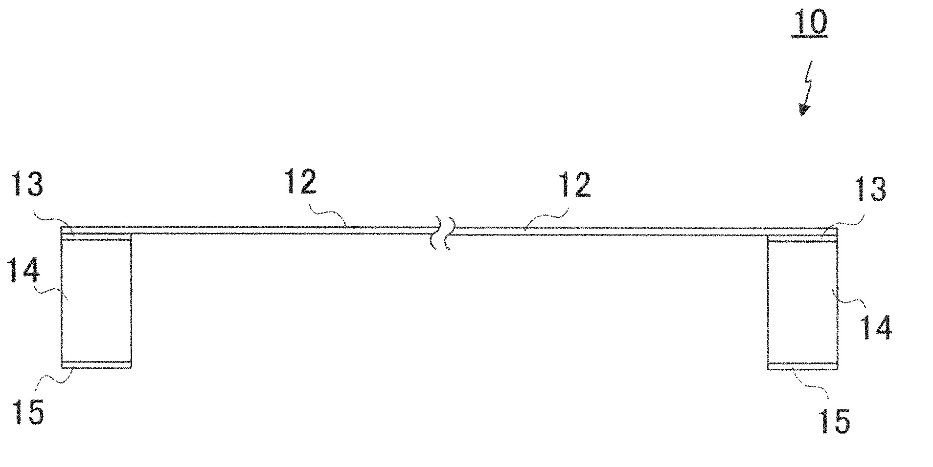
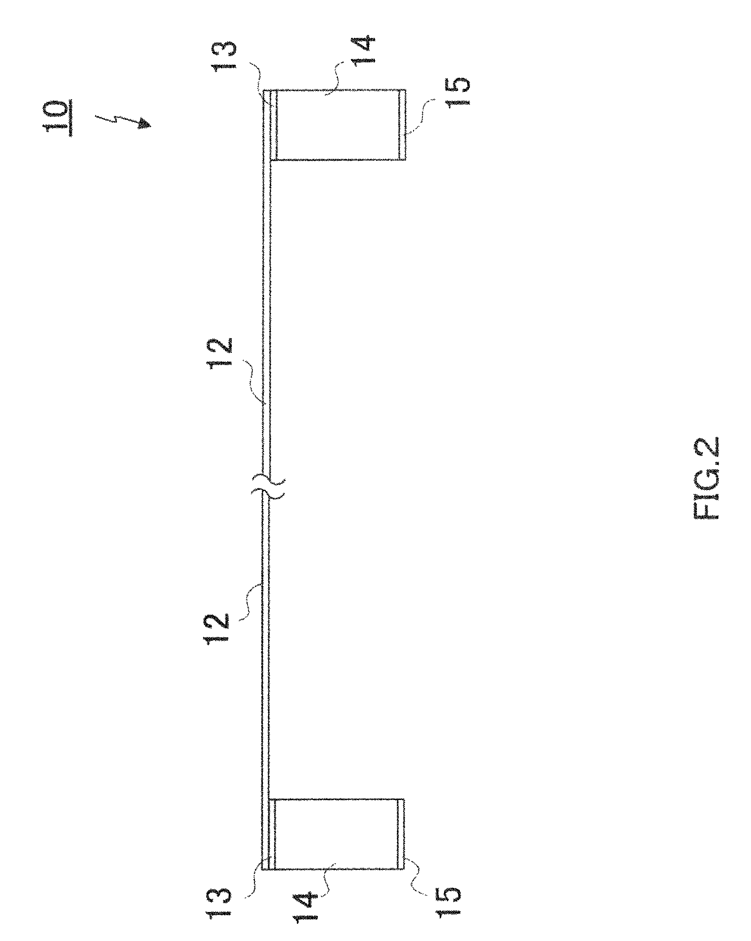
Pellicle and mask adhesive therefor
a mask adhesive and pellicle technology, applied in the field of pellicle and mask adhesive therefor, can solve the problems of inability to obtain desired pattern, limited microfabrication of pattern, size, quality and appearance of pattern, etc., and achieve the effect of not deformed or distorted, less adhesive residue, and appropriate softness
- Summary
- Abstract
- Description
- Claims
- Application Information
AI Technical Summary
Benefits of technology
Problems solved by technology
Method used
Image

Examples
example 1
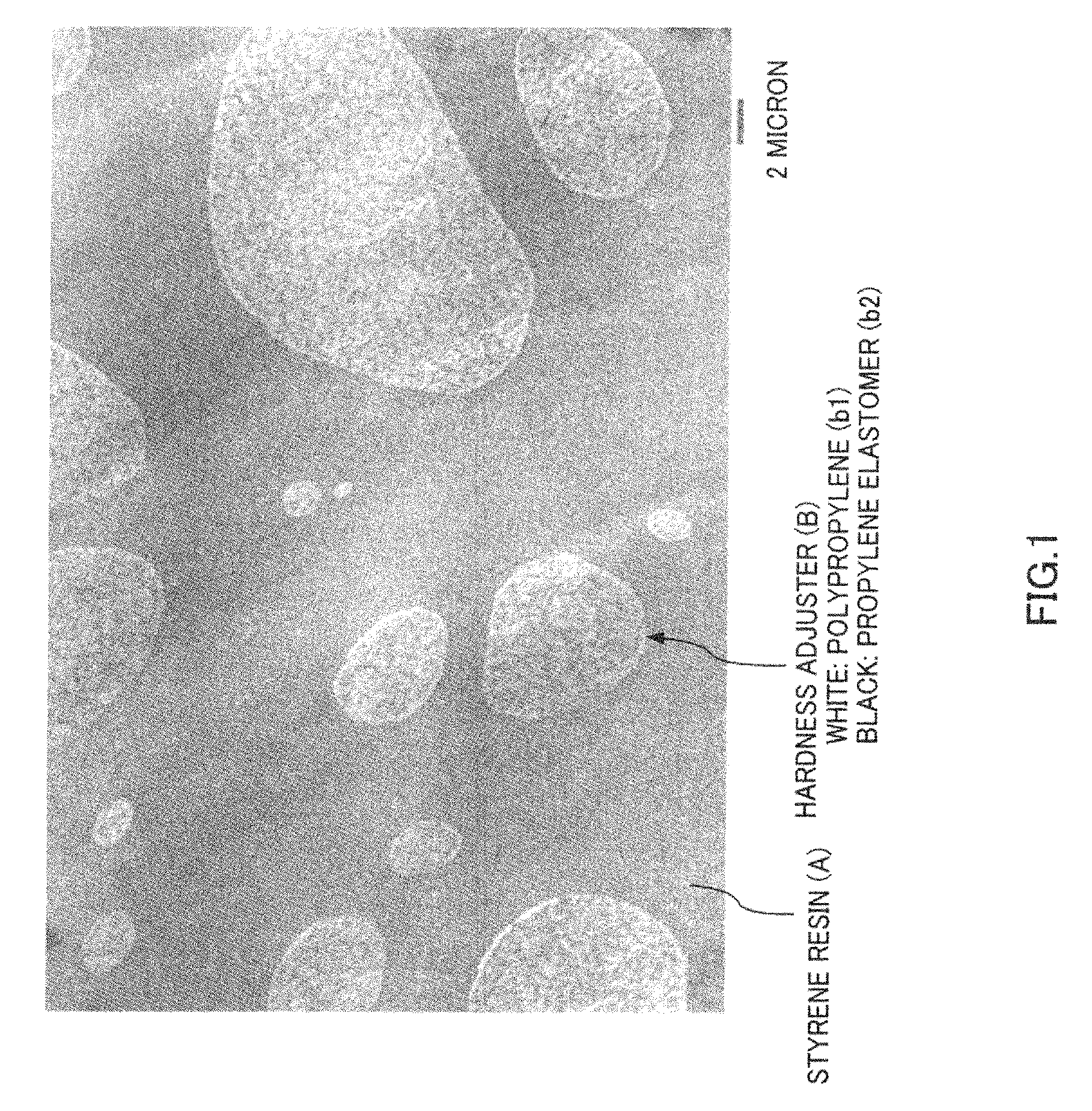
[0117]SEBS shown below as a styrene resin (A), a mixture of the random polypropylene (b1) and a propylene-butene-ethylene copolymer (b2) shown below as a hardness adjuster (B), polybutene (NISSAN polybutene 30N, NOF Corporation) as a softener (C), and ARKON P100 (Arakawa Chemical Industries, Ltd.) as a tackifier (D), are measured and mixed with the compounding ratio (mass ratio) shown in Table 1 (FIG. 4) to a total of 48 g.
[0118](A) Styrene Resin
[0119]SEBS (TOUGH TECH®H1221, Asahi Kasei Chemicals Corporation)
[0120]Content of a styrene-derived unit: 12 mass %
[0121]Maximum value of tan δ at −30° C.: 2.0
[0122]Solubility parameter (SP value): 16.7 (J / cm3)1 / 2
[0123](B) Hardness Adjuster
[0124]A 15 / 85 (mass ratio) mixture of the random polypropylene (b1) and the propylene-butene-ethylene copolymer (b2).
[0125]Maximum value of tan δ at −20° C.: 1.0
[0126]Storage elastic modulus at 25° C.: 1.1×10⁷ Pa·s
[0127](b1) Random polypropylene (C2 / C3 mol %=1 / 99)
[0128]Storage elastic modulus at 25° C.: 3×...
examples 2 to 4
[0139]Mask adhesives are prepared in the same way as in Example 1 except for using different compounding ratios shown in Table 1. Pellicles are made using these mask adhesives in the same way as in Example 1.
example 5
[0140]A mask adhesive is prepared in the same way as in Example 1 except for using polybutene (NISSO-PB hydrogen additive type PB resin GI2000, Nippon Soda Co., Ltd.) as a softener (C), and using the different compounding ratio shown in Table 1. A pellicle is made using this mask adhesive in the same way as in Example 1.
PUM
| Property | Measurement | Unit |
|---|---|---|
| width | aaaaa | aaaaa |
| width | aaaaa | aaaaa |
| tensile elastic modulus | aaaaa | aaaaa |
Abstract
Description
Claims
Application Information