Method for manufacturing semiconductor device

a semiconductor device and manufacturing technology, applied in the field of methods, can solve the problems of low heat resistance, glass substrate cannot be heated at a temperature which exceeds the upper temperature limit, process temperature limitations, etc., and achieve the effect of large area and crystallinity recovery

Inactive Publication Date: 2014-07-08
SEMICON ENERGY LAB CO LTD
View PDF108 Cites 22 Cited by
  • Summary
  • Abstract
  • Description
  • Claims
  • Application Information

AI Technical Summary

Benefits of technology

[0014]In view of such problems, an object of the present invention is to provide a method for manufacturing a semiconductor substrate, by which a high-performance semiconductor element can be formed even when a substrate having low heat resistance is used as a supporting substrate.
[0038]By a method for manufacturing a semiconductor substrate of the present invention, a single crystal semiconductor layer which is obtained by being separated from a single crystal semiconductor substrate can be recrystallized by being heated at a process temperature of 700° C. or less, and its crystallinity can be recovered. In addition, the single crystal semiconductor layer which is obtained by being separated from the single crystal semiconductor substrate can be planarized at a process temperature of 700° C. or less. Therefore, even if a substrate having low heat resistance is used as a supporting substrate, a high-performance semiconductor element can be formed by using a semiconductor substrate. For example, by using a light-transmitting glass substrate having a large area, a high-performance display device can be formed.

Problems solved by technology

However, a glass substrate has a strain point of 700° C. or lower and thus has low heat resistance.
Therefore, a glass substrate cannot be heated at a temperature which exceeds its upper temperature limit, and the process temperature is limited to be 700° C. or lower.
That is, there are also limitations on process temperatures for a step of removing a crystal defect at a separation plane and a step of planarizing a surface.
Removal of a crystal defect in a semiconductor layer that is bonded to a silicon wafer has been conventionally achieved by heating at a temperature of 1000° C. or higher; however, such a high temperature process cannot be employed for removal of a crystal defect in a semiconductor layer that is bonded to a glass substrate having a strain point of 700° C. or lower.
That is, a re-single-crystallization method has not been established, by which a single crystal semiconductor layer that is bonded to a glass substrate having a strain point of 700° C. or less is recovered to a single crystal semiconductor layer having the same or substantially the same crystallinity as a single crystal semiconductor substrate before processing.
In particular, it is difficult to perform treatment by mechanical polishing on a large-area glass substrate having a side that is longer than 30 cm.
Thus, if there is a large unevenness of the semiconductor layer, it is difficult to manufacture a gate insulating layer with high dielectric strength.
Accordingly, large unevenness on the surface of the semiconductor layer causes a decrease in performance of the semiconductor elements such as a decrease in field effect mobility, an increase in threshold voltage, and the like.
In this manner, when a substrate which has low heat resistance and is easily bent, such as a glass substrate, is used as a supporting substrate, a problem emerges in that it is difficult to improve surface unevenness of a semiconductor layer that is separated from a silicon wafer and fixed to the supporting substrate.

Method used


Image

  • Method for manufacturing semiconductor device
  • Method for manufacturing semiconductor device
  • Method for manufacturing semiconductor device

Examples


embodiment mode 1

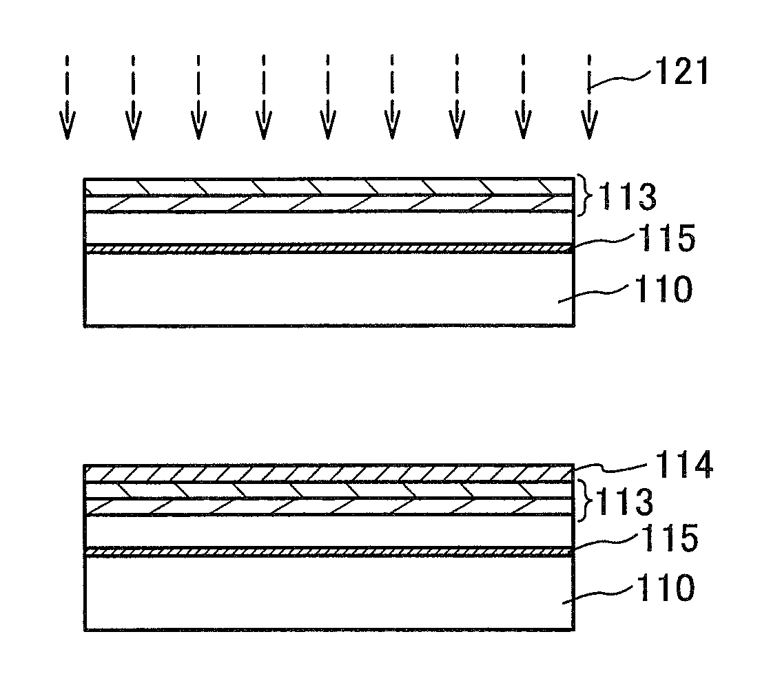
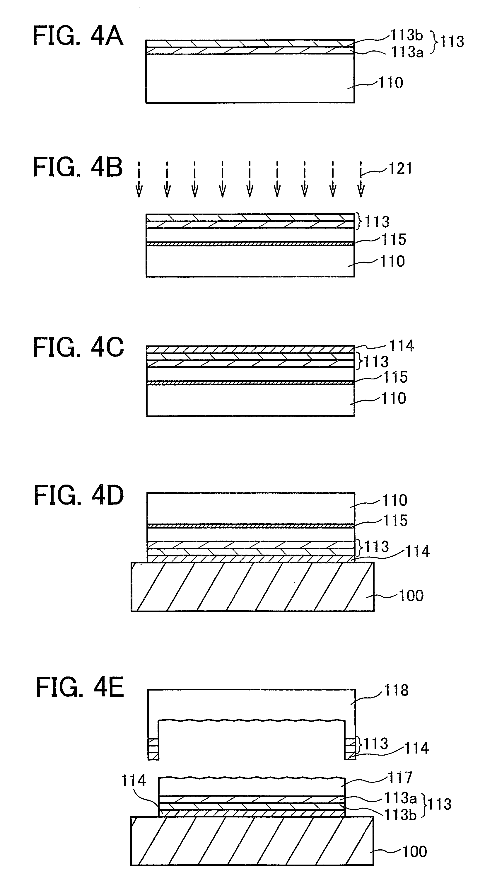
[0089]In this embodiment mode, a semiconductor substrate in which a single crystal semiconductor layer is fixed to a supporting substrate with a buffer layer interposed therebetween and a manufacturing method thereof will be described.

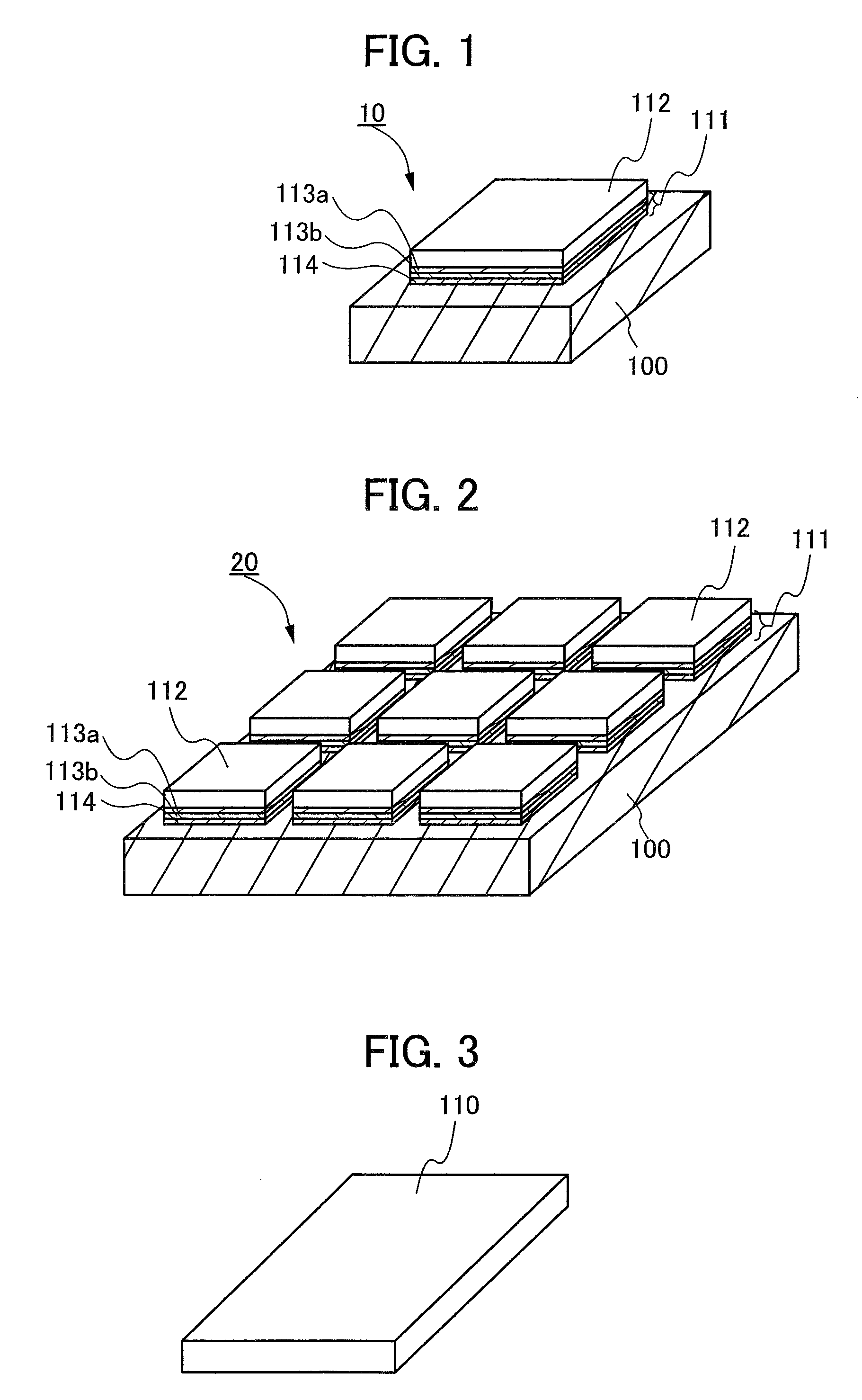
[0090]FIG. 1 shows a perspective view of an example of a structure of a semiconductor substrate. In a semiconductor substrate 10, a single crystal semiconductor layer 112 is fixed to a supporting substrate 100 with a buffer layer 111 interposed therebetween. The single crystal semiconductor layer 112 is formed by thinning of a single crystal semiconductor substrate. The single crystal semiconductor layer 112 is fixed to the supporting substrate 100 by bonding of the surface of the buffer layer 111 and the surface of the supporting substrate 100 to each other. The semiconductor substrate 10 is a substrate having a so-called SOI structure, in which a single crystal semiconductor layer is formed over an insulating layer.

[0091]The buffer layer 111 may have...

embodiment mode 2

[0239]In this embodiment mode, a semiconductor substrate in which a single crystal semiconductor layer is fixed to a supporting substrate with a buffer layer interposed therebetween and a manufacturing method thereof will be described. In this embodiment mode, a method for manufacturing a semiconductor substrate in which a buffer layer is formed over a supporting substrate will be described.

[0240]FIG. 6 shows a perspective view of an example of a structure of a semiconductor substrate. In a semiconductor substrate 30, a single crystal semiconductor layer 112 is bonded to a supporting substrate 100. The single crystal semiconductor layer 112 is formed by thinning of a single crystal semiconductor substrate and is fixed to the supporting substrate 100 with a buffer layer 111 and a buffer layer 101 interposed therebetween. The semiconductor substrate 30 is a substrate having a so-called SOI structure, in which a single crystal semiconductor layer is formed over an insulating layer. The...

embodiment mode 3

[0280]In this embodiment mode, a laser irradiation apparatus with which a single crystal semiconductor layer is irradiated with a laser beam while being heated is described. FIG. 11 shows an example of a structure of the laser irradiation apparatus.

[0281]As shown in FIG. 11, the laser irradiation apparatus includes a laser 301 that emits a laser beam 300 and a stage 303 where an object 302 is disposed. The laser 301 is connected to a controller 304. By the control of the controller 304, energy of the laser beam 300 emitted from the laser 301, repetition rate, or the like can be changed. The stage 303 is provided with a heating device such as a resistance heating device or the like, with which the object 302 can be heated.

[0282]The stage 303 is provided so that the stage 303 can move inside the chamber 306. An arrow 307 indicates a direction of movement of the stage 303.

[0283]A window 308 through which the laser beam 300 is guided into the chamber 306 is provided in the wall of the c...


PUM

PropertyMeasurementUnit
temperatureaaaaaaaaaa

Abstract

A single crystal semiconductor substrate is irradiated with ions that are generated by exciting a hydrogen gas and are accelerated with an ion doping apparatus, thereby forming a damaged region that contains a large amount of hydrogen. After the single crystal semiconductor substrate and a supporting substrate are bonded, the single crystal semiconductor substrate is heated to be separated along the damaged region. While a single crystal semiconductor layer separated from the single crystal semiconductor substrate is heated, this single crystal semiconductor layer is irradiated with a laser beam. The single crystal semiconductor layer undergoes re-single-crystallization by being melted through laser beam irradiation, thereby recovering its crystallinity and planarizing the surface of the single crystal semiconductor layer.

Description

BACKGROUND OF THE INVENTION[0001]1. Field of the Invention[0002]The present invention relates to a method for manufacturing a semiconductor substrate to which a single crystal semiconductor layer is fixed with a buffer layer interposed therebetween and a method for manufacturing a semiconductor device.[0003]2. Description of the Related Art[0004]In recent years, integrated circuits using a silicon-on-insulator (SOI) substrate instead of a bulk silicon wafer have been developed. A feature of a thin single crystal silicon layer formed over an insulating layer can be taken advantage of to form a completely electrically isolated semiconductor layer of a transistor in an integrated circuit and to form a completely depleted transistor. Accordingly, a semiconductor integrated circuit having high added values such as high integration, high-speed operation, and low power consumption can be realized.[0005]Known examples of SOI substrates are SIMOX substrates and bonded substrates. For example...

Claims


Application Information

Patent Timeline
Patent Type & Authority Patents(United States)
IPC IPC(8): H01L21/762
CPCH01L27/1266B23K26/03B23K26/083B23K26/12B23K26/127B23K26/14H01L21/268H01L21/3247H01L21/76254H01L27/1214H01L29/66772H01L27/1218H01L21/20H01L21/324
Inventor YAMAZAKI, SHUNPEIMOMO, JUNPEIISAKA, FUMITOHIGA, EIJIKOYAMA, MASAKISHIMOMURA, AKIHISA
Owner SEMICON ENERGY LAB CO LTD
Why Eureka
Try Eureka