Method and apparatus for a lateral radiation detector
a radiation detector and lateral technology, applied in the field of radiation detectors, can solve the problems that the leakage current level still does not meet the stringent requirements of high-sensitivity and low-noise indirect conversion x-rays
- Summary
- Abstract
- Description
- Claims
- Application Information
AI Technical Summary
Benefits of technology
Problems solved by technology
Method used
Image
Examples
first embodiment
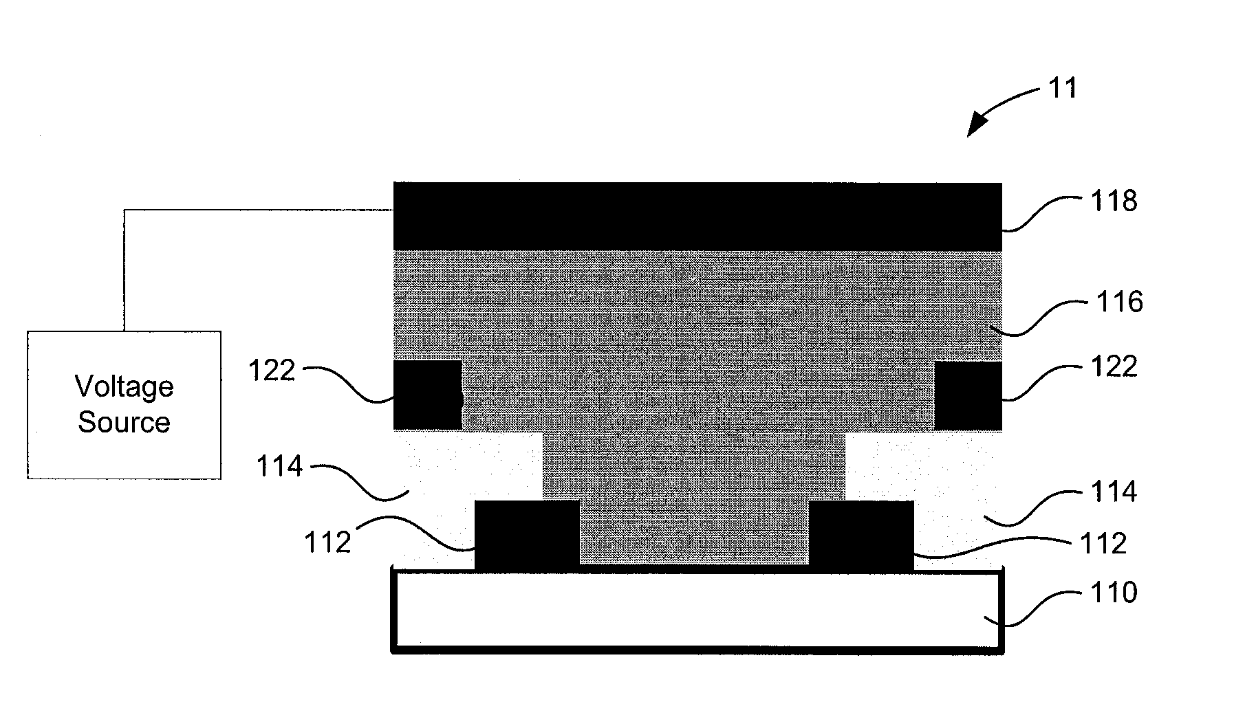
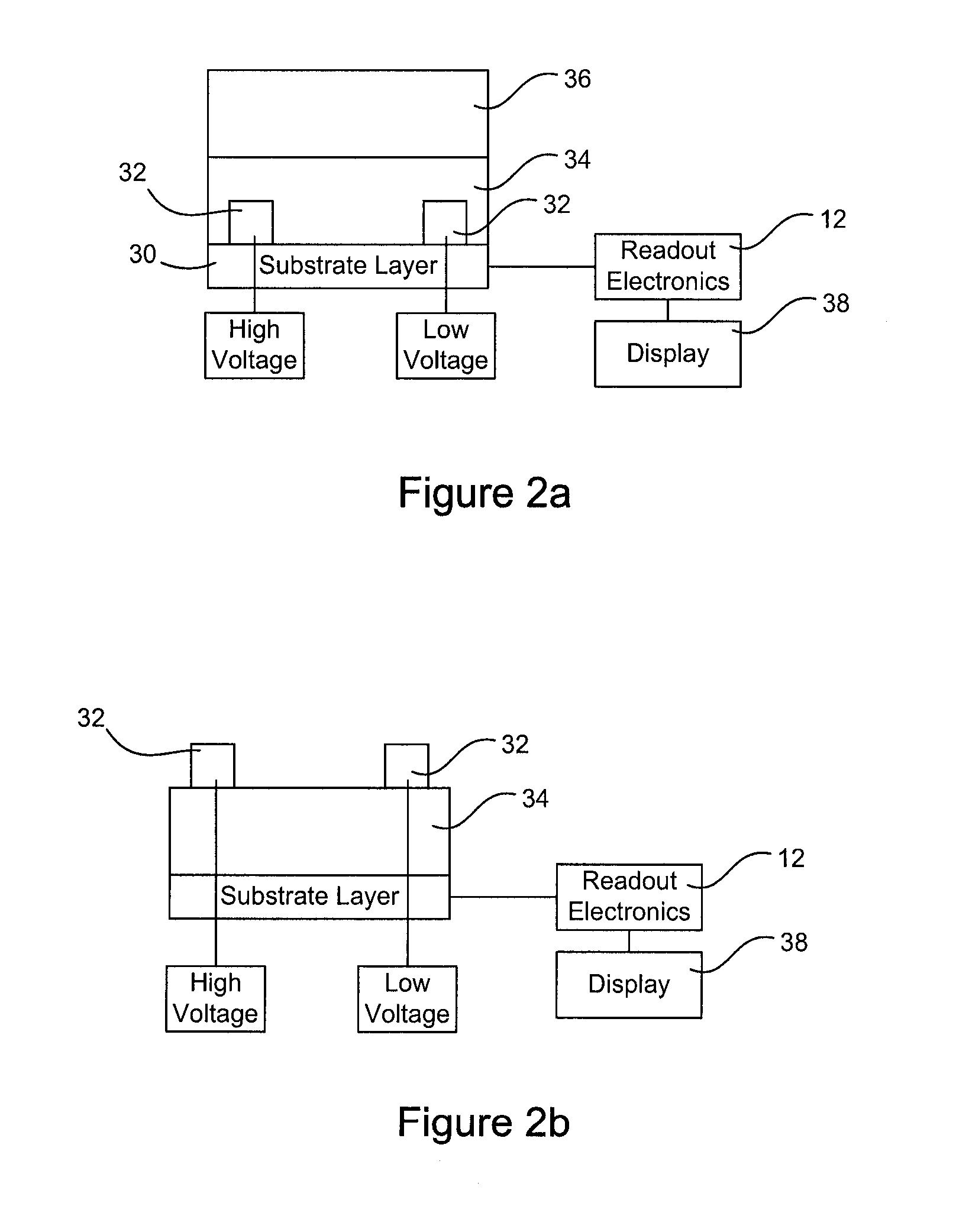
[0036]Turning to FIG. 2a, a more detailed schematic view of the radiation detector 11 is shown. In the current embodiment, the radiation detector 11 is a photoconductive-type photodetector (PD) or a lateral PD. The radiation detector 11 includes a substrate layer 30 such as a thin film transistor (TFT) array or a CMOS electron pixilated array. Other substrate layers are contemplated and will be understood by those skilled in the art.
[0037]Atop the substrate layer 30 are a set of contacts 32 made of a metal such as aluminum or the like. The contacts 32 can also be seen as electrodes with at least one of the contacts being a cathode and at least one of the contacts being an anode. In the current embodiment, the contacts 32 are located directly on top of the substrate layer 30 and are laterally spaced apart from each other. Although the set of contacts 32 are shown to be at extreme opposite ends from each other, the spacing between the contacts is determined by the applications for whi...
second embodiment
[0039]Turning to FIG. 2b, a schematic view of a lateral radiation detector 11 is shown. In this embodiment, the detector 11 includes a substrate layer 30 which is connected to the readout electronics 12, which, in turn, are connected to the display 38. On top of the substrate layer 30 is a photoconductor layer 34 such as a-Se, with a set of contacts 32, laterally spaced from each other, located on top of the photoconductor layer 34. In operation, the radiation detector 11 of FIG. 2b is preferably used with a tri-layer bottom gate staggered thin film transistor. Alternatively, the set of contacts 32 can be located in a top portion of the photoconductor layer 34 (FIG. 2c) or adjacent the photoconductor layer 34 (FIG. 2d). The voltage sources 33a and 33b are connected to the electrodes 32 to provide the necessary electric field for in which the high energy photons travel.
[0040]In each embodiment, the contacts 32 are preferably implemented using a finger or spiral shape.
[0041]Turning to...
PUM
 Abstract
Description
Claims
Application Information


