Optical semiconductor, optical semiconductor electrode using same, photoelectrochemical cell, and energy system

a technology of optical semiconductor and electrode, applied in the field of optical semiconductor, optical semiconductor electrode using same, photoelectrochemical cell, energy system, can solve the problems of difficult to further reduce the band gap of insub>z, and only 1% sunlight can be used, and achieves small band gap, high quantum efficiency, and high carrier mobility

Active Publication Date: 2014-10-07
PANASONIC CORP
View PDF10 Cites 1 Cited by
  • Summary
  • Abstract
  • Description
  • Claims
  • Application Information

AI Technical Summary

Benefits of technology

[0016]The optical semiconductor of the present invention is a solid solution of InN, GaN and ZnO having a wurtzite crystalline phase, and has a crystalline phase, at least a part of which has a stable wurtzite structure. In addition, the optical semiconductor of the present invention has an In-richer composition than conventional nitride semiconductors composed of a solid solution of GaN and InN. Therefore, the optical semiconductor of the present invention has a smaller band gap and can utilize visible light. Furthermore, since the optical semiconductor of the present invention has high carrier mobility, it is an excellent semiconductor having high quantum efficiency. For these reasons, the optical semiconductor of the present invention, for example, can utilize sunlight effectively and has optical semiconductor properties with high quantum efficiency.
[0017]In the optical semiconductor electrode of the present invention, the composition B having the same composition as the optical semiconductor of the present invention is used as a material for the surface near-field region of the optical semiconductor layer. This allows the optical semiconductor electrode of the present invention to have the same effects as those obtained by the optical semiconductor of the present invention. In addition, the composition A is used for the junction plane near-field region with the conductive substrate of the optical semiconductor layer. The composition A is an oxide containing Ga, In and Zn, in which oxygen is not substituted by nitrogen, and has a higher Fermi level than the composition B. Thus, the optical semiconductor layer containing both the composition A and the composition B has improved charge separation capability. As a result, its quantum efficiency is further improved.
[0018]The first and second photoelectrochemical cells of the present invention utilize the optical semiconductor of the present invention. The first and second photoelectrochemical cells of the present invention can improve the quantum efficiency of the hydrogen evolution reaction by irradiation with light by the effects obtained by the optical semiconductor of the present invention. Since the energy system of the present invention is provided with such a photoelectrochemical cell, efficient electric power supply is achieved.

Problems solved by technology

Therefore, the semiconductor electrode disclosed in Patent Literature 1 has a problem in that only about 1% of sunlight can be utilized.
Therefore, it is difficult to further reduce the band gap of InzGa1-zN by increasing the content of In.

Method used


Image

  • Optical semiconductor, optical semiconductor electrode using same, photoelectrochemical cell, and energy system
  • Optical semiconductor, optical semiconductor electrode using same, photoelectrochemical cell, and energy system
  • Optical semiconductor, optical semiconductor electrode using same, photoelectrochemical cell, and energy system

Examples


first embodiment

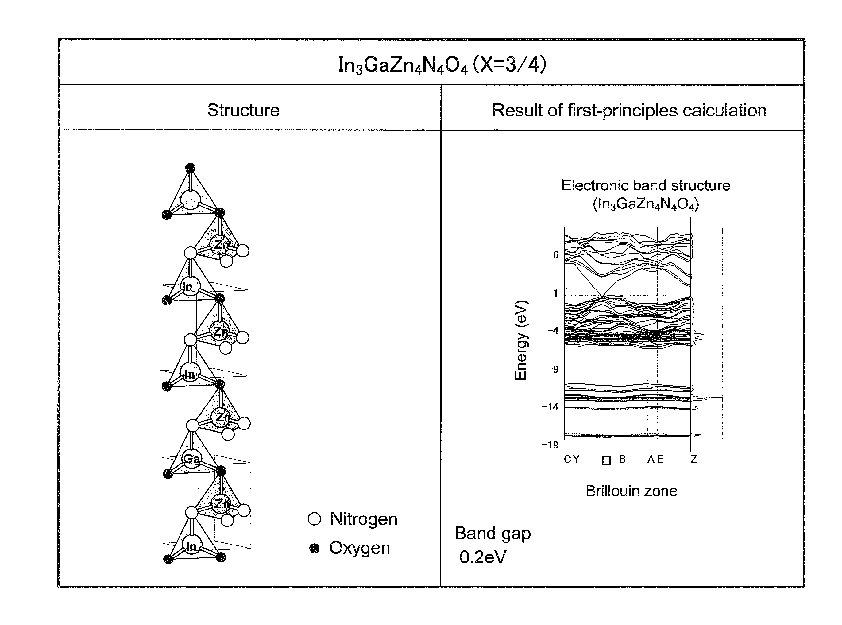
[0035]The optical semiconductor of the first embodiment of the present invention is an optical semiconductor containing In, Ga, Zn, O and N, and has a composition in which a part of O is substituted by N in a general formula: In2xGa2(1-x)O3(ZnO)y, where x and y satisfy 0.2

[0036]The optical semiconductor having such a composition is a solid solution of InN, GaN and ZnO having a wurtzite crystalline phase, and has a crystalline phase, at least a part of which has a stable wurtzite structure. In addition, since this optical semiconductor has an In-rich composition with a high content of In, it has a smaller band gap than conventional optical semiconductors composed of a single crystal solid solution (InzGa1-zN) of GaN and InN. For these reasons, this optical semiconductor is an optical semiconductor having excellent semiconductor characteristics, and for example, it can utilize sunlight effectively and exhibit optical semiconductor properties with high quantum efficiency...

second embodiment

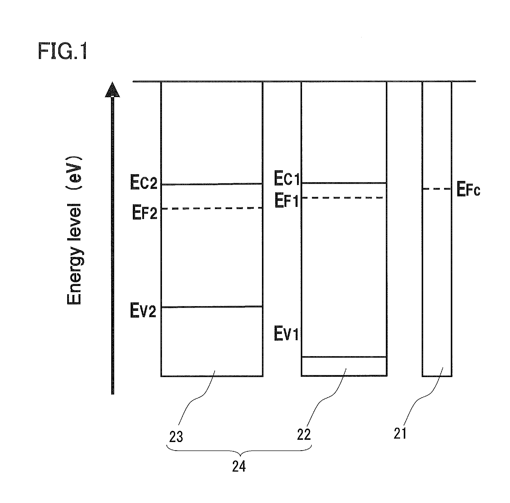
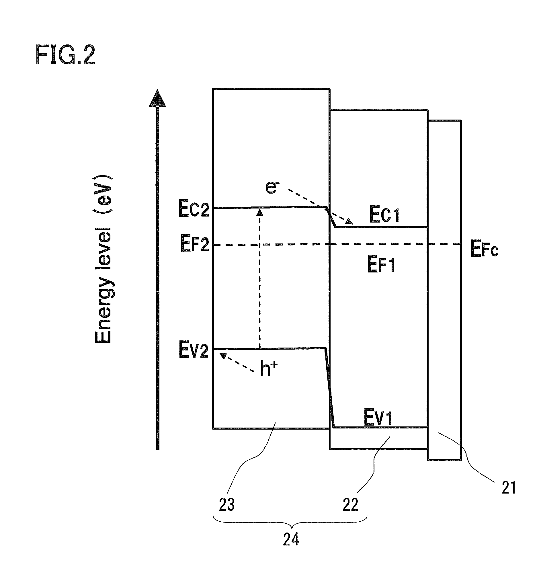
[0046]The optical semiconductor electrode of the present invention includes a conductive substrate and an optical semiconductor layer disposed on the conductive substrate. In the optical semiconductor layer, the junction plane near-field region of the optical semiconductor layer with the conductive substrate is composed of the composition A represented by a general formula: In2xGa2(1-x)O3(ZnO)y, where x and y satisfy 0.2

[0047]In the optical semiconductor electrode of t...

third embodiment

[0057]A photoelectrochemical cell according to an embodiment of the present invention is described.

[0058]The photoelectrochemical cell of the present embodiment includes an optical semiconductor electrode, a counter electrode, a water-containing electrolyte, and a container containing these. The optical semiconductor electrode includes a conductive substrate and an optical semiconductor layer disposed on the conductive substrate and containing the optical semiconductor of the present invention as described in the first embodiment. The counter electrode is connected electrically to the conductive substrate of the optical semiconductor electrode. The electrolyte is in contact with the surfaces of the optical semiconductor layer and the counter electrode. The photoelectrochemical cell generates hydrogen when the optical semiconductor layer is irradiated with light.

[0059]Since this configuration causes charge separation to occur in the photoexcited optical semiconductor, the quantum eff...


PUM

PropertyMeasurementUnit
lengthaaaaaaaaaa
inner diameteraaaaaaaaaa
lengthaaaaaaaaaa

Abstract

The optical semiconductor of the present invention is an optical semiconductor containing In, Ga, Zn, O and N, and has a composition in which a part of oxygen (O) is substituted by nitrogen (N) in a general formula: In2xGa2(1-x)O3(ZnO)y, where x and y satisfy 0.2<x<1 and 0.5≦y. In the general formula, x is preferably 0.5, and furthermore, y is preferably 1 or more and 6 or less, and more preferably 2 or 6. It is preferred that the optical semiconductor of the present invention have a wurtzite crystal structure. The optical semiconductor of the present invention is an excellent optical semiconductor because it has a smaller band gap, can utilize visible light, and has high carrier mobility and thus has high quantum efficiency.

Description

TECHNICAL FIELD[0001]The present invention relates to an optical semiconductor for decomposing water by irradiation with light, an optical semiconductor electrode and a photoelectrochemical cell each using the same, and an energy system using the photoelectrochemical cell.BACKGROUND ART[0002]Conventionally, it is known that a semiconductor material that functions as an optical semiconductor decomposes water into hydrogen and oxygen when the semiconductor material is irradiated with light (see, for example, Patent Literature 1). Patent Literature 1 discloses a technique in which an n-type semiconductor electrode and a counter electrode are disposed in an electrolyte and the surface of the n-type semiconductor electrode is irradiated with light, so that hydrogen and oxygen are obtained from the surfaces of both electrodes. Specifically, the use of a TiO2 electrode or the like as the n-type semiconductor electrode is described therein.[0003]However, the band gap of TiO2 (anatase type) ...

Claims


Application Information

Patent Timeline
Patent Type & Authority Patents(United States)
IPC IPC(8): H01L29/12C01B21/082C25B1/00H01M8/06
CPCH01M8/0656C01B21/0821C25B1/003Y02E60/366C01P2002/85C01P2002/84C01P2002/77C01P2002/72Y02E60/50Y02E60/364C04B35/453C04B35/58C04B35/62675C04B2235/3284C04B2235/3286C04B2235/46C04B2235/76C04B2235/80C04B2235/81C25B1/55Y02E60/36
Inventor NOMURA, TAKAIKISUZUKI, TAKAHIROMIYATA, NOBUHIROHATO, KAZUHITO
Owner PANASONIC CORP
Why Eureka
Try Eureka