Device containing plurality of smaller MEMS devices in place of a larger MEMS device

a technology of mems devices and devices, which is applied in the direction of acceleration measurement using interia forces, printed circuit non-printed electric components association, instruments, etc., can solve the problems of inability to seal such devices in cavities, pressure on the roof of cavities, and inability to achieve capacitance resolution

Active Publication Date: 2014-10-14
QORVO US INC
View PDF26 Cites 14 Cited by
  • Summary
  • Abstract
  • Description
  • Claims
  • Application Information

AI Technical Summary

Benefits of technology

[0135]Advantages of the present invention include the capability to have fully integrated packaging into the BEOL of a semiconductor process as opposed to a separate package that is required now and noise immunity from the small size of each switch. Each switch in the array has a higher resonant frequency compared to a single large MEMS device, and so is less prone to vibration noise at low frequencies. Another advantage is integrated analog to digital conversion since the sampled switch count (digital) represents the magnitude of the input signal (analog). Another advantage is decreased cost over competing solutions because it can be embedded in the back end and does not need a separate package. Another advantage includes the device can be integrated with standard ICs because it can be encapsulated in the back end processing, which is not possible with the existing larger single MEMS devices.

Problems solved by technology

It is then very difficult to seal such a device in a cavity using the typical interlayer dielectrics found in the back end or the metallization found in the back end because these are of the order of 1 micron thick.
A low pressure cavity is usually required for the operation of these devices, which leads to a pressure on the roof of the cavity.
In some applications it would be advantageous to have a MEMS device on the same chip as a micro controller or other logic device, but that is not possible because it must be separately packaged.
These complex packaging strategies add to the cost of the sensor and limit the sensors ability to be fully integrated in a standard back and of the line (BEOL) or standard packaging flow.

Method used


Image

  • Device containing plurality of smaller MEMS devices in place of a larger MEMS device
  • Device containing plurality of smaller MEMS devices in place of a larger MEMS device
  • Device containing plurality of smaller MEMS devices in place of a larger MEMS device

Examples


Embodiment Construction

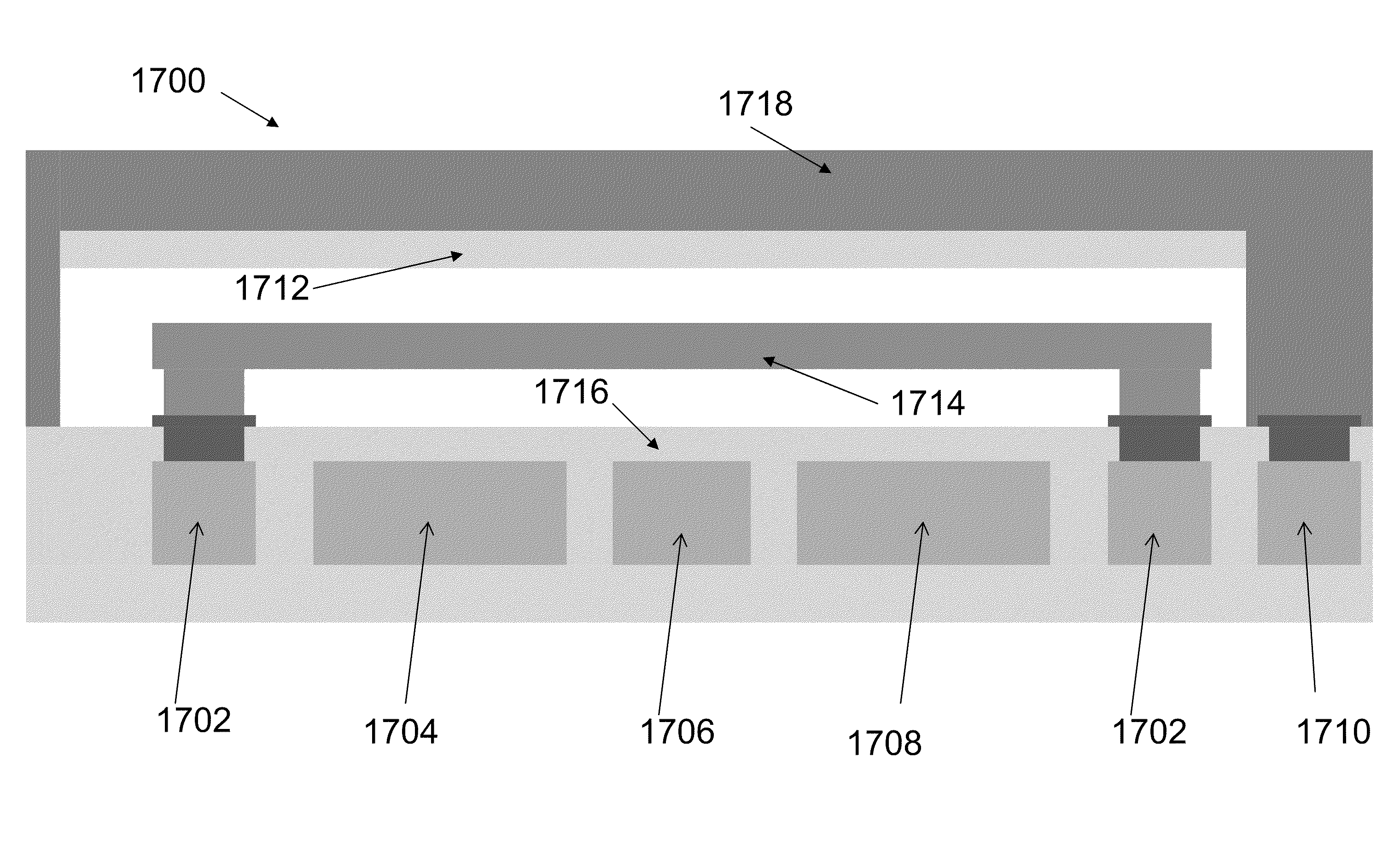
[0037]Embodiments discussed herein generally include using a large number of small MEMS devices to replace the function of an individual larger MEMS device or a digital variable capacitor. Solutions discussed herein include breaking up a single MEMS device or a variable capacitor into an array of smaller MEMS devices that perform the same function as the single larger MEMS device variable capacitor. Each individual MEMS device in the array may only be a few microns across and so can be housed in a cavity that fits within the back end metallization. The roof of the cavity can be 1 micron thick interlayer dielectric for example, and because it is only a few microns wide, the atmospheric pressure outside is not large enough to cause any significant deformation of the cavity roof, even for an evacuated cavity.

[0038]To illustrate why an array of small MEMS devices acting to measure some physical phenomena has an advantage over a single large MEMS device, some of the embodiments discussed...


PUM


Abstract

Embodiments disclosed herein generally include using a large number of small MEMS devices to replace the function of an individual larger MEMS device or digital variable capacitor. The large number of smaller MEMS devices perform the same function as the larger device, but because of the smaller size, they can be encapsulated in a cavity using complementary metal oxide semiconductor (CMOS) compatible processes. Signal averaging over a large number of the smaller devices allows the accuracy of the array of smaller devices to be equivalent to the larger device. The process is exemplified by considering the use of a MEMS based accelerometer switch array with an integrated analog to digital conversion of the inertial response. The process is also exemplified by considering the use of a MEMS based device structure where the MEMS devices operate in parallel as a digital variable capacitor.

Description

CROSS-REFERENCE TO RELATED APPLICATIONS[0001]This application claims benefit of U.S. Provisional Patent Application Ser. No. 61 / 112,521, filed Nov. 7, 2008, which is herein incorporated by reference.BACKGROUND OF THE INVENTION[0002]1. Field of the Invention[0003]Embodiments of the present invention generally relate to a device and a method of using the device where a plurality of smaller micro-electromechanical system (MEMS) devices replace a single, larger MEMS device.[0004]2. Description of the Related Art[0005]MEMS devices are routinely produced using semiconductor processing. This allows accelerometers, pressure sensors, low resistance current switches or RF switches, variable capacitance devices, resonators and other devices to be manufactured cheaply. For many of these devices to work with the desired physical properties they usually cover an area of several hundred microns square. It is then very difficult to seal such a device in a cavity using the typical interlayer dielect...

Claims


Application Information

Patent Timeline
Patent Type & Authority Patents(United States)
IPC IPC(8): H05K1/18B81B7/04G01P15/08G01P15/125G01P15/135G01P15/18H01G5/18H01G5/40
CPCB81B7/04H01G5/40G01P15/135H01G5/18G01P15/125G01P15/0802B81B2201/0221B81B2201/0235B81B2207/053
Inventor SMITH, CHARLES GORDONKNIPE, RICHARD L.JOSHI, VIKRAMGADDI, ROBERTOUNAMUNO, ANARTZVAN KAMPEN, ROBERTUS PETRUS
Owner QORVO US INC
Why Eureka
Try Eureka