Semiconductor external cavity laser with integrated planar waveguide bragg grating and wide-bandwidth frequency modulation

a planar waveguide and laser technology, applied in the field of narrowlinewidth external cavity lasers, can solve the problems of limiting the application of direct current modulation fm approach, unable to procure high frequency modulation at a specified laser wavelength, and inability to achieve external frequency modulation. , to achieve the effect of wide bandwidth, extending frequency modulation, and negligible phase delay

Active Publication Date: 2014-11-11
OPTASENSE
View PDF7 Cites 15 Cited by
  • Summary
  • Abstract
  • Description
  • Claims
  • Application Information

AI Technical Summary

Benefits of technology

[0016]The present invention describes narrow-linewidth semiconductor external cavity laser (ECL) with integrated wide bandwidth (BW) intracavity frequency modulation (FM) section. The laser is preferably packaged in a standard form-factor package, such as a 14-pin butterfly package. The front end of the cavity comprises an integrated planar circuit (e.g., silica-on-silicon planar lightwave circuit with Bragg gratings), and the “back facet” of the laser is implemented as a high-reflection (HR) coated lithium niobate (LiNbO3) phase tuning section in the double pass configuration. AC-voltage signal applied

Problems solved by technology

As soon as laser is locked, “external” frequency modulation is not possible any more.
This design addresses slow but wide wavelength tuning over a C-band but fails to procure a high frequency modulation at a specified laser wavelength.
Due to the thermal time constants of the gain chip, FM is associated with large phase delay, which limits applications of direct curr

Method used


Image

  • Semiconductor external cavity laser with integrated planar waveguide bragg grating and wide-bandwidth frequency modulation
  • Semiconductor external cavity laser with integrated planar waveguide bragg grating and wide-bandwidth frequency modulation
  • Semiconductor external cavity laser with integrated planar waveguide bragg grating and wide-bandwidth frequency modulation

Examples


first embodiment

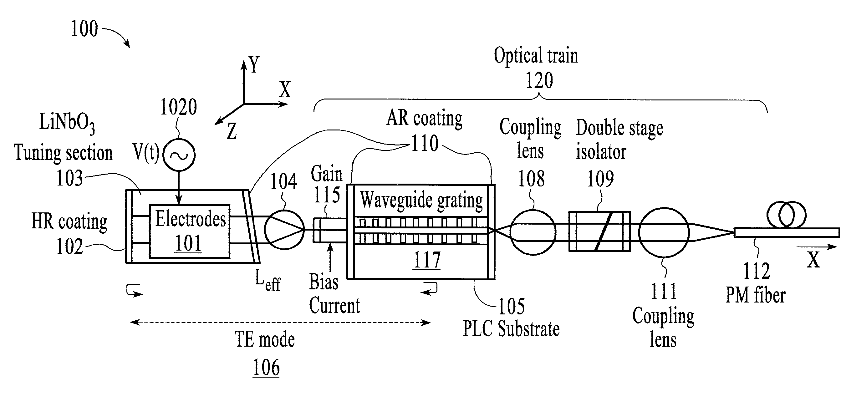
[0029]FIG. 1 shows the present invention. This embodiment provides an external cavity arrangement having frequency modulation with uniform frequency response and wide bandwidth (up to 100 MHz), and at the same time, maintains desirable properties, such as narrow linewidth and low frequency noise.

[0030]To meet such requirements, this embodiment uses a hybrid architecture of the external cavity where a high reflectivity back facet is formed by a LiNbO3 bulk crystal in double pass configuration, and an antireflection (AR)-coated semiconductor gain element coupled to the back face through a micro lens (ball or aspheric types).

[0031]The front end of the external cavity, similar to what is described in US2010 / 0303121, is formed by a gain element butt-coupled to the dispersive Bragg grating formed in polarization maintaining PLC waveguide. Such front end of the external cavity maintains all essential elements of PLANEX-type design which combines integration of the semiconductor gain chip w...

second embodiment

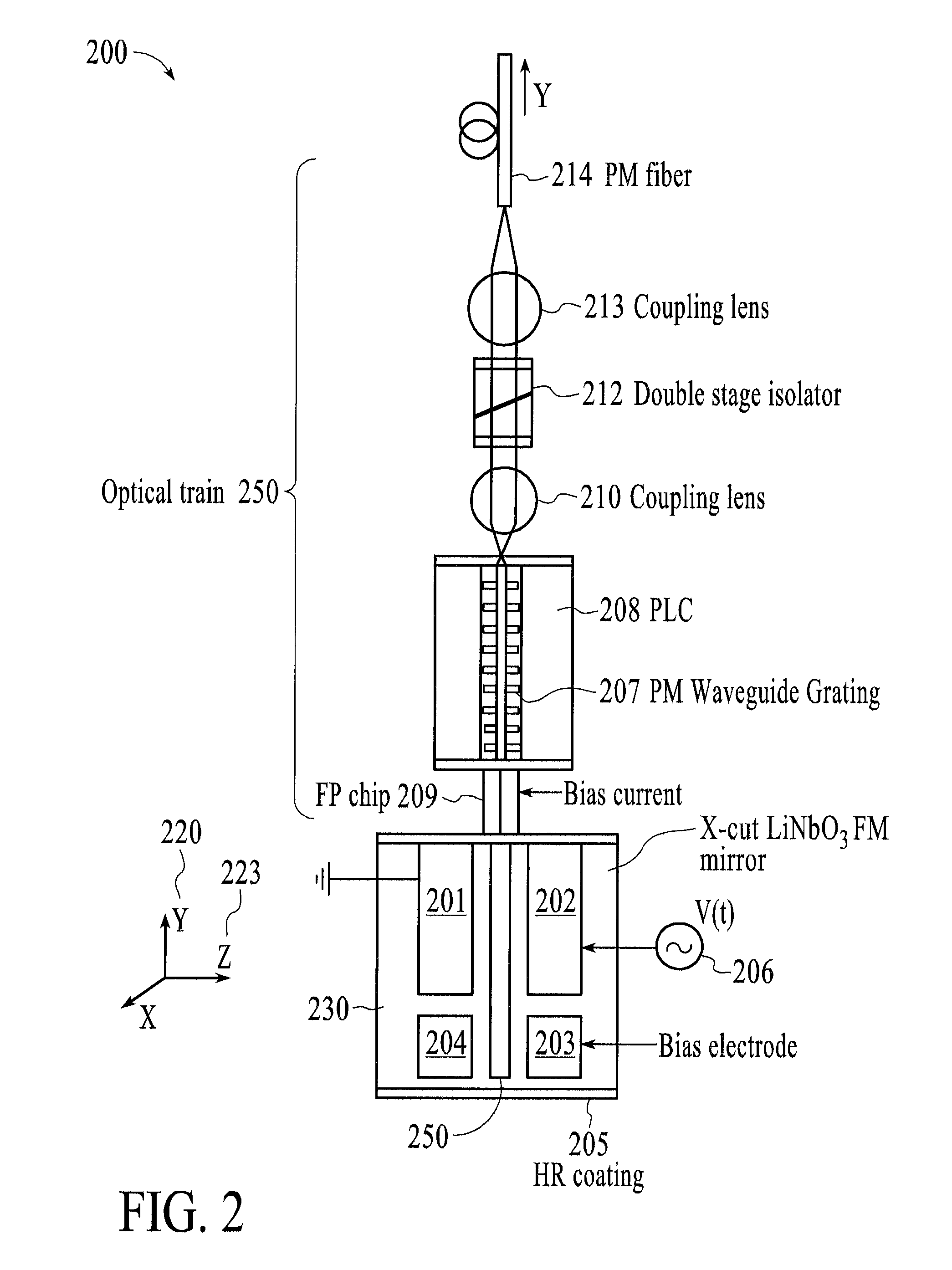
[0033]the invention provides an external cavity laser with low voltage requirements to produce frequency modulation with uniform amplitude and phase response. Such an external cavity use a PLANEX-type optical architecture as the front end while the back facet of such cavity is implemented by a LiNbO3 waveguide in double pass configuration, as shown in the configuration in FIG. 2. To achieve requirements for low applied voltage, embodiments of the present invention utilize LiNbO3 mirror in the form of X-cut crystal orientation waveguide located between two pairs of deposited electrodes. A first pair of RF electrodes is used for frequency modulation. A second pair of electrodes is used as DC-bias electrodes and enables fine DC-adjustment of the phase of an external cavity independently of bias current of Fabry-Perot (FP) chip without inducing any thermal effect, as the current is low.

[0034]In the above embodiment, the waveguide is located between the electrodes and utilizes the orient...

third embodiment

[0052]the present invention provides a hybrid external cavity FM laser assembled to be packaged in a standard form-factor package, such as a 14-pin butterfly package. FIG. 6-7 show two views of such an embodiment. In this embodiment, the “back facet” includes a free-space LiNbO3 FM phase section attached to a heat spreader substrate, a semiconductor chip with a thermoelectric cooler (TEC), V-grove alignment fixture, a coupling micro-lens and AR-coated Fabry-Perot (FP) gain chip assembly. Using proper design to extend over the phase section, the TEC chip helps to stabilize modulation performance and alignment stability of LiNbO3 FM phase section.

[0053]FIG. 6 (and the magnified backend 700 shown in FIG. 7) describe a 14-pin telecom packaging assembly 600 which includes extended semiconductor thermoelectric cooler (TEC) 601, substrate with heat spreader 604 and integration of the external cavity elements including Fabry-Perot (FP) gain chip 701, PLC waveguide grating 603, and free-spac...


PUM


Abstract

The present disclosure describes semiconductor external cavity laser with wide bandwidth frequency modulation capabilities. The laser is preferably packaged in a standard form-factor package, such as a 14-pin butterfly package. The front end of the cavity comprises an integrated planar circuit (e.g., silica-on-silicon planar lightwave circuit with Bragg gratings), and the “back facet” of the laser is implemented as a high-reflection (HR) coated LiNbO3 phase tuning section in the double pass configuration. AC-voltage signal applied to the electrodes of phase tuning section modulates a refractive index of the propagating TE-polarization mode of external cavity and produces frequency modulation. Such frequency modulation is not associated with any thermal behavior of the gain element included in the external cavity laser, and has a negligible phase delay over a wide bandwidth.

Description

CROSS-REFERENCE TO RELATED APPLICATIONS[0001]This application claims priority from U.S. Provisional Patent Application Ser. No. 61 / 540,466 filed Sep. 28, 2011, which is incorporated herein by reference.FIELD OF THE INVENTION[0002]The present invention relates to narrow-linewidth external cavity lasers (ECL) with a wide-bandwidth (BW) intra-cavity frequency modulating section integrated into the design of the laser.BACKGROUND[0003]There are different known approaches to accomplish wavelength tuning and / or frequency modulation (FM) using an electro optical material such as lithium niobate (LiNbO3).[0004]U.S. Pat. No. 5,384,799 describes a semiconductor gain element which is coupled to and frequency locked to surface acoustic modes generated by an acousto-optical transducer located at a front facet of a compound external cavity of a laser. Such frequency locking served only “internal” purposes to produce a highly coherent laser with narrow linewidth. As soon as laser is locked, “extern...

Claims


Application Information

Patent Timeline
IPC IPC(8): H01S5/10H01S3/10
CPCH01S5/10H01S5/02216H01S5/141H01S5/02284H01S5/0064H01S3/107H01S5/02252H01S5/02438H01S5/005H01S5/02415H01S5/0287H01L2224/48091H01S5/02326H01S5/02251H01L2924/00014H01S5/146
Inventor KUPERSHMIDT, VLADIMIRSTOLPNER, LEWALALUSI, MAZINLI, STEVE YIQIANG
Owner OPTASENSE
Why Eureka
Try Eureka