Check patentability & draft patents in minutes with Patsnap Eureka AI!

Light-emitting device with an insulating partition

a technology of light-emitting devices and partitions, which is applied in the direction of static indicating devices, thermoelectric devices, instruments, etc., can solve the problems of color conversion efficiency, power consumption in color filter power consumption in color conversion methods is higher than that in separate coloring methods, so as to increase the definition and the size of a substrate. , the effect of manufacturing in simple steps

Inactive Publication Date: 2014-11-18
SEMICON ENERGY LAB CO LTD
View PDF16 Cites 10 Cited by
  • Summary
  • Abstract
  • Description
  • Claims
  • Application Information

AI Technical Summary

Benefits of technology

The present invention provides a low-power light-emitting device that can be made in simple steps and increase the definition and size of a substrate. This device can be used in electronic devices. A method is employed to form a color filter or color conversion layer between the first electrode layer and the substrate using a highly-conducting wiring, which simplifies the manufacturing process and reduces costs. The use of an active-matrix light-emitting device structure with a transistor as a switching element and a first electrode layer connected to the source or drain electrode layer of the transistor facilitates improvement in image quality and reduces power consumption. The device contains a donor substance, such as alkali metals, alkaline earth metals, rare earth metals, or their compounds, which increases the conductivity of the layer containing organic compounds. This invention provides a simple yet efficient solution for producing high-quality light-emitting devices.

Problems solved by technology

However, power consumption in the color filter method is higher than that in the separate coloring method because light is absorbed by a color filter, which is problematic.
In addition, power consumption in the color conversion method is higher than that in the separate coloring method because color conversion efficiency is not always 100%, which is problematic.

Method used


Image

  • Light-emitting device with an insulating partition
  • Light-emitting device with an insulating partition
  • Light-emitting device with an insulating partition

Examples


embodiment 1

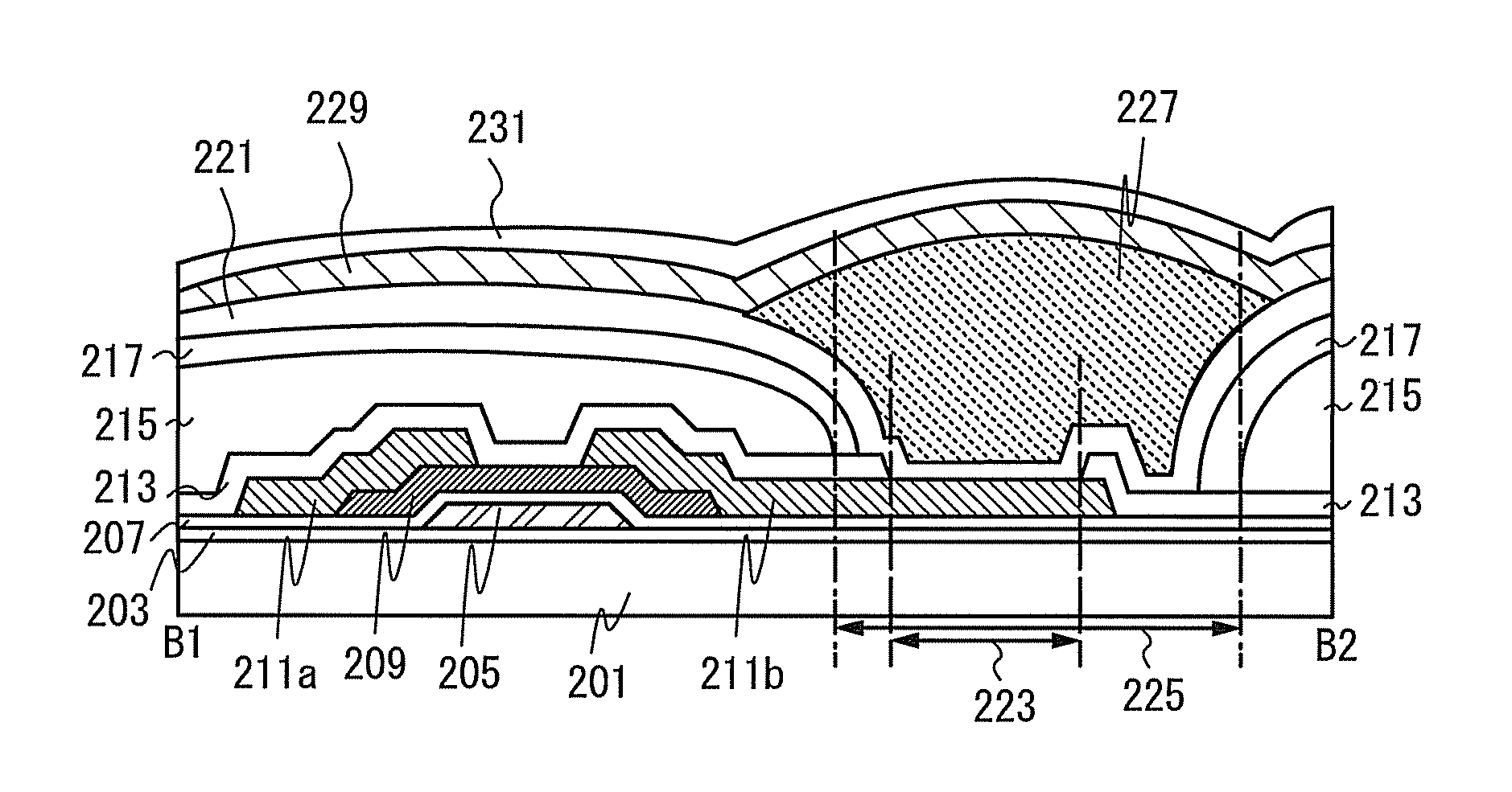
[0038]In this embodiment, a light-emitting device in one embodiment of the present invention is described with reference to FIG. 1, FIG. 2, FIGS. 3A and 3B, FIGS. 4A and 4B, and FIG. 5.

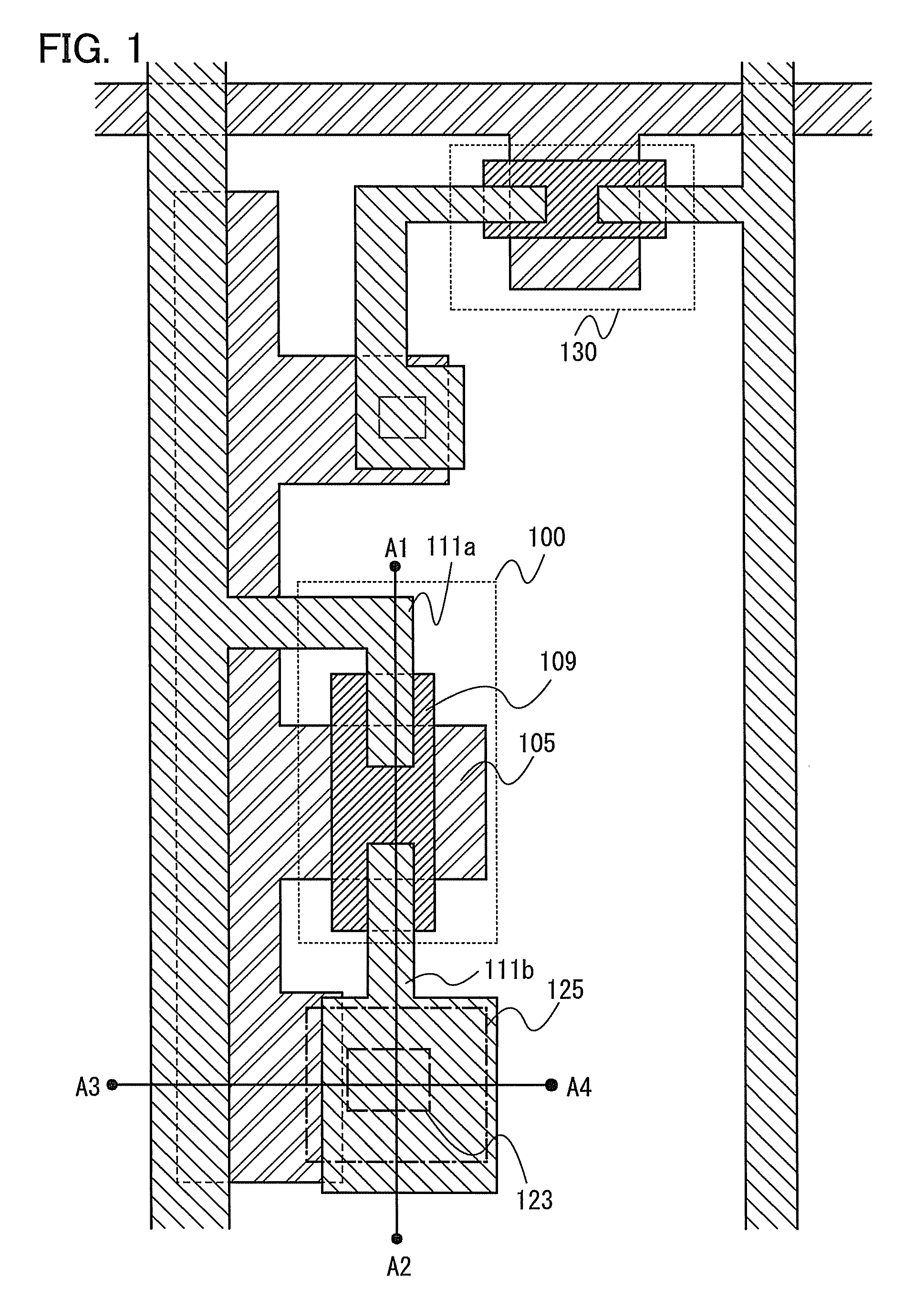
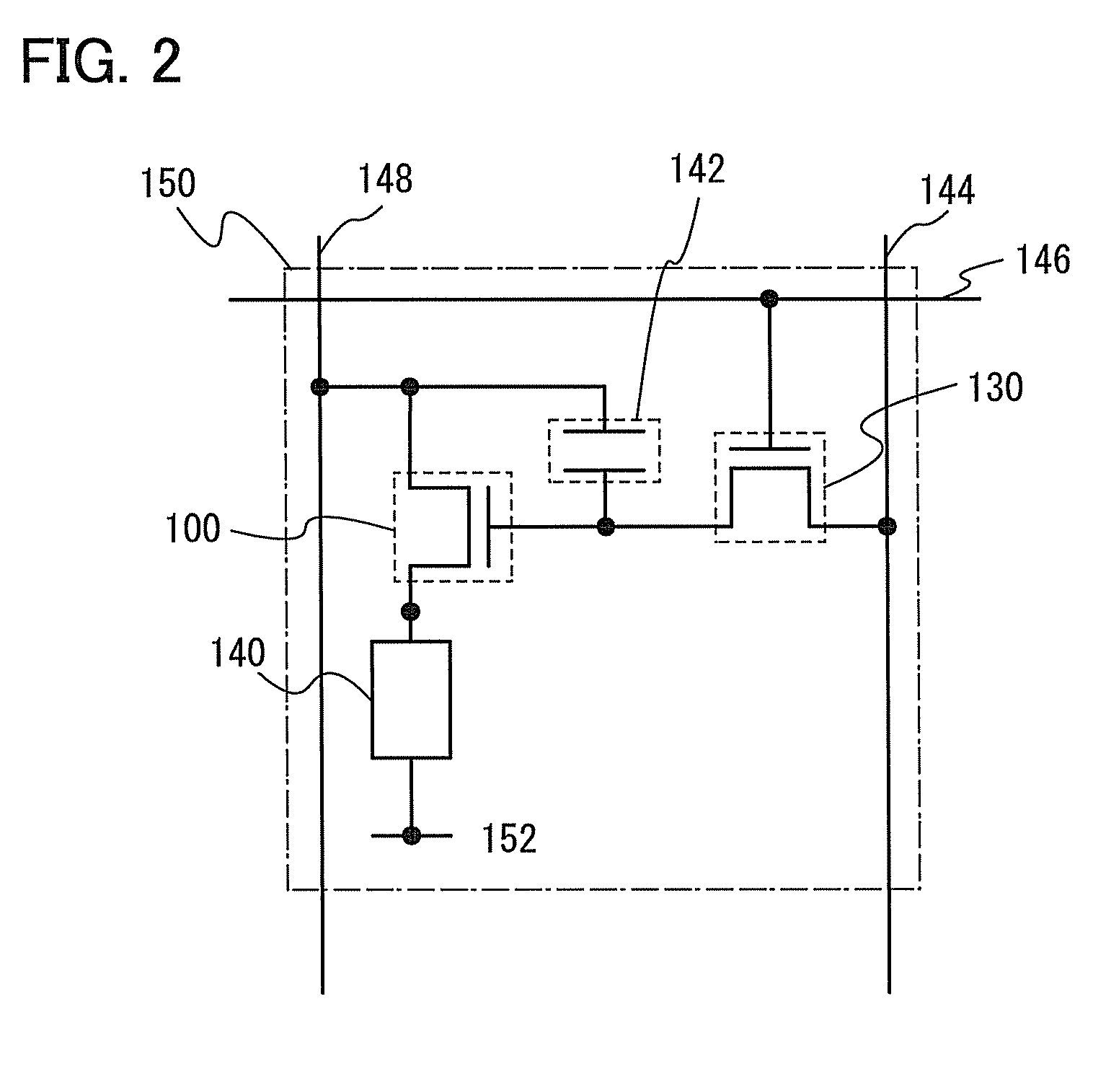
[0039]FIG. 1 is the top view of a pixel portion of the light-emitting device in one embodiment of the present invention. The light-emitting device illustrated in FIG. 1 includes a drive transistor 100 and a switching transistor 130. The drive transistor 100 includes a gate electrode layer 105, an oxide semiconductor layer 109 that is a semiconductor layer, and a source and drain electrode layers 111a and 111b. FIG. 2 corresponds to an equivalent circuit of a circuit of the pixel portion illustrated in FIG. 1.

[0040]FIG. 2 illustrates an example of a pixel structure of the light-emitting device in one embodiment of the present invention to which digital time-ratio grayscale driving can be applied.

[0041]The structure and operation of a pixel to which digital time-ratio grayscale driving can be applied ar...

embodiment 2

[0063]In this embodiment, an example of a method for manufacturing the light-emitting device in Embodiment 1 is described with reference to FIGS. 6A to 6C.

[0064]First, the base layer 103 is formed over the substrate 101 for transmitting visible light. Since the substrate 101 is positioned in a direction in which light from the EL layer is extracted, a material for transmitting visible light, for example, glass such as barium borosilicate glass or aluminoborosilicate glass, plastics, a polyester film, or an acrylic film is used for the substrate 101. The base layer 103 has a function of preventing diffusion of impurities from the substrate 101; however, the base layer 103 is not necessarily provided. The base layer can be formed to have a single-layer structure or a layered structure including a silicon nitride film, a silicon oxide film, a silicon nitride oxide film, and a silicon oxynitride film.

[0065]First, a conductive film is formed over the base layer 103. Then, the gate electr...

embodiment 3

[0127]In this embodiment, an example of an EL layer used in a light-emitting device in one embodiment of the present invention is described with reference to FIG. 7. An EL layer described in this embodiment can be used as the EL layer 129 (see FIG. 3A and FIG. 4A) and the EL layer 229 (see FIG. 3B and FIG. 4B) in Embodiment 1.

[0128]The EL layer 129 in this embodiment that is illustrated in FIG. 7 is provided between the pair of electrodes (the first electrode layer 121 and the second electrode layer 131). A region 1120 where the first electrode layer 121 is in direct contact with the EL layer 129 and overlaps with the second electrode layer 131 is a desired light-emitting region. The EL layer 129 includes a hole injection layer 1111, a hole transport layer 1112, a light-emitting layer 1113, an electron transport layer 1114, and an electron injection layer 1115 as functional layers. Note that the first electrode layer 121 and the second electrode layer 131 may be formed using the mat...


PUM

PropertyMeasurementUnit
frequencyaaaaaaaaaa
thicknessaaaaaaaaaa
thicknessaaaaaaaaaa

Abstract

A low-power light-emitting device which can be manufactured in simple steps and is suitable for increasing definition and the size of a substrate is provided. The light-emitting device includes a layer for blocking visible light; a conductive layer that partly overlaps with the layer for blocking visible light; a color filter layer that includes an opening over the layer for blocking visible light; a first electrode layer for transmitting visible light that is connected to the conductive layer through the opening, over the color filter layer; an insulating partition over the first electrode layer overlapping with the opening; a layer containing an organic compound over the first electrode layer and the partition; and a second electrode layer over the layer containing an organic compound. The layer containing an organic compound includes a layer containing a donor substance and an acceptor substance and a layer containing a light-emitting organic compound.

Description

BACKGROUND OF THE INVENTION[0001]1. Field of the Invention[0002]The present invention relates to light-emitting devices and electronic devices including layers containing organic compounds as light-emitting layers.[0003]2. Description of the Related Art[0004]Light-emitting elements including organic compounds as luminous bodies, which have features of thinness, lightness, high-speed response to input signals, and DC drive at low power supply voltage, have been expected to be applied to next-generation flat panel displays or lighting devices. In particular, display devices in which light-emitting elements are arranged in matrix have been considered to have advantages of a wide viewing angle and high visibility over conventional liquid crystal display devices.[0005]The emission mechanism of a light-emitting element including an organic compound as a luminous body is as follows. First, when voltage is applied between a pair of electrodes with an electroluminescence (hereinafter also re...

Claims


Application Information

Patent Timeline
Patent Type & Authority Patents(United States)
IPC IPC(8): H01L51/50H01L33/00H01L29/04H01L27/32G02F1/136H01L51/52H05B44/00
CPCH01L27/3246H01L51/5284H01L51/5052H01L27/3248H01L27/322H01L51/5278H10K59/38H10K59/123H10K59/122H10K50/155H10K50/165H10K50/19H10K59/8792H10K50/865
Inventor ARASAWA, RYO
Owner SEMICON ENERGY LAB CO LTD
Features
  • R&D
  • Intellectual Property
  • Life Sciences
  • Materials
  • Tech Scout
  • Unparalleled Data Quality
  • Higher Quality Content
  • 60% Fewer Hallucinations
Learn More