
Vertical group III-V nanowires on si, heterostructures, flexible arrays and fabrication

a nanowire and heterostructure technology, applied in the field of integrated group iiiv, can solve the problems of less than straightforward integration, higher cost of iii-v materials, and more complex fabrication, and achieve the effect of reducing the distance and high optical absorption

Active Publication Date: 2015-01-13
RGT UNIV OF CALIFORNIA
View PDF10 Cites 20 Cited by
  • Summary
  • Abstract
  • Description
  • Claims
  • Application Information

AI Technical Summary

Benefits of technology

The invention provides a way to grow vertical semiconductor nanowires on silicon, starting with a complete removal of native oxide from the silicon surface. The silicon substrate is then placed in a chamber and heated while a gas containing III-V precursors flows through it. The resulting structure has no tapered nanowires and contains a core-shell structure with complementary doping in the shell. This structure has high optical absorption and reduces the distance over which carriers must diffuse before being collected. This method allows for the growth of complex semiconductor patterns on silicon, which could improve the performance and efficiency of semiconductor devices.

Problems solved by technology

Silicon remains the industry standard for the electronics industry standard, however, because the Group III-V materials are higher cost, involve more complex fabrication and are not as widely available as silicon.
The different material systems have incompatibilities that make the integration less than straightforward.
The presence of Au additionally can cause unwanted deep level traps in the silicon layer upon which the nanowires are formed.
Self-catalyzed growth of III-V nanowires on silicon is a simpler technique, but reported methods do not provide control over the orientation of the nanowires that form.

Method used


Image

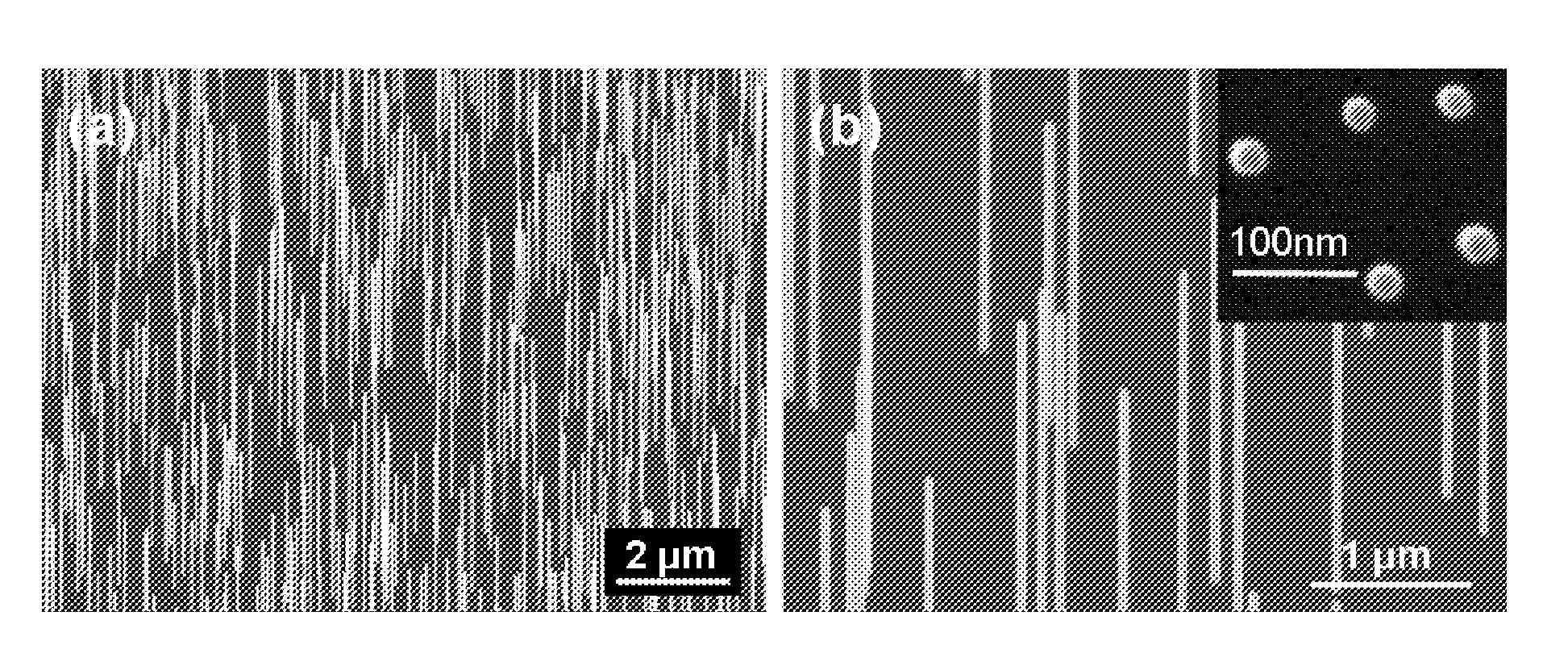
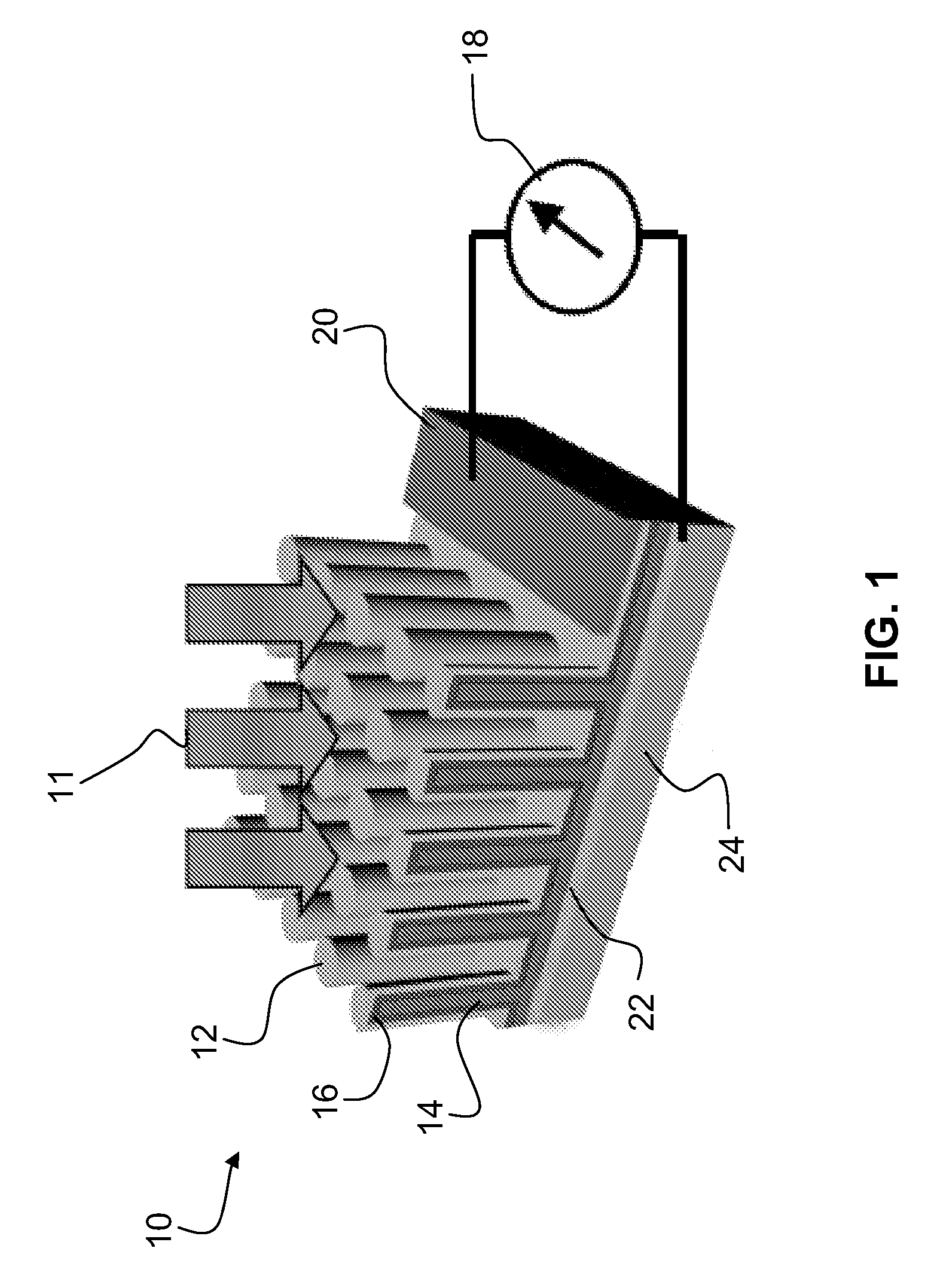
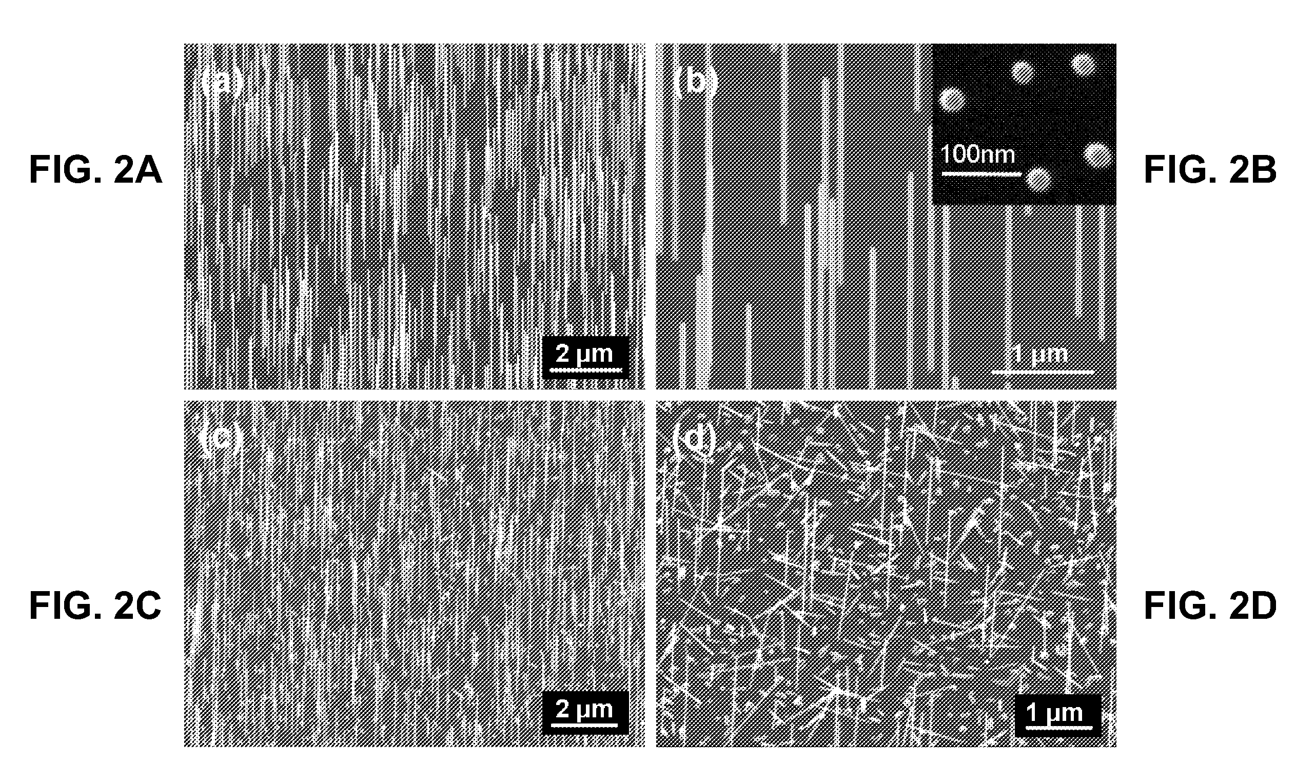
  • Vertical group III-V nanowires on si, heterostructures, flexible arrays and fabrication
  • Vertical group III-V nanowires on si, heterostructures, flexible arrays and fabrication
  • Vertical group III-V nanowires on si, heterostructures, flexible arrays and fabrication

Examples


Embodiment Construction

[0021]Embodiments of the invention provide for the direct epitaxial ground of Group III-V semiconductors on silicon with fewer processing steps than typical past methods, which keeps the silicon relatively uncontaminated but consistently produces vertical nanowire growth. Preferred methods of the invention provide vertical epitaxial growth of III-V nanowires on a silicon substrate over a large area using Metal-Organic Chemical Vapor Deposition (MOCVD). No pre-deposited material (e.g., metal catalyst, oxide template) is required to accomplish the nanowire growth in accordance with the invention, which significantly simplifies the growth process and eliminates undesirable effects associated with such steps. The invention provides reliable methods that are the basis for low-cost, high-volume fabrication. Methods of the invention allow direct integration of functional III-V-nanowire structures into Si-based microelectronics / photonics. This enables fabrication of devices that combine und...


PUM

PropertyMeasurementUnit
temperatureaaaaaaaaaa
view angleaaaaaaaaaa
temperatureaaaaaaaaaa

Abstract

Embodiments of the invention provide a method for direct heteroepitaxial growth of vertical III-V semiconductor nanowires on a silicon substrate. The silicon substrate is etched to substantially completely remove native oxide. It is promptly placed in a reaction chamber. The substrate is heated and maintained at a growth temperature. Group III-V precursors are flowed for a growth time. Preferred embodiment vertical Group III-V nanowires on silicon have a core-shell structure, which provides a radial homojunction or heterojunction. A doped nanowire core is surrounded by a shell with complementary doping. Such can provide high optical absorption due to the long optical path in the axial direction of the vertical nanowires, while reducing considerably the distance over which carriers must diffuse before being collected in the radial direction. Alloy composition can also be varied. Radial and axial homojunctions and heterojunctions can be realized. Embodiments provide for flexible Group III-V nanowire structures. An array of Group III-V nanowire structures is embedded in polymer. A fabrication method forms the vertical nanowires on a substrate, e.g., a silicon substrate. Preferably, the nanowires are formed by the preferred methods for fabrication of Group III-V nanowires on silicon. Devices can be formed with core / shell and core / multi-shell nanowires and the devices are released from the substrate upon which the nanowires were formed to create a flexible structure that includes an array of vertical nanowires embedded in polymer.

Description

REFERENCE TO RELATED APPLICATIONS AND PRIORITY CLAIM[0001]This application claims priority under 35 U.S.C. §119 and all other applicable statutes and treaties from prior U.S. provisional application Ser. No. 61 / 108,979, filed on Oct. 28, 2008 and from prior U.S. provisional application Ser. No. 61 / 183,726, filed on Jun. 3, 2009.STATEMENT OF GOVERNMENT INTEREST[0002]This invention was made with government support under grant no. DE-FG36-08GO018016 awarded by Department of Energy and under grant no. ECS0506902 awarded by the National Science Foundation. The government has certain rights in the invention.FIELD[0003]A field of the invention is integrated Group III-V (arsenide, phosphide, nitride, heterostructures, homostructures and alloys) and silicon devices and fabrications. Example applications of integrated Group III-V / silicon devices of the invention include nanowire-based solar cells, light-emitting diodes (LEDs), lasers, photodetectors and sensors, field-effect transistors (FETs...

Claims


Application Information

Patent Timeline
Patent Type & Authority Patents(United States)
IPC IPC(8): H01L21/20B82Y10/00H01L21/02H01L27/06H01L29/06H01L29/20H01L29/205H01L29/267H01L29/778H01L29/88H01L31/0352H01L31/074H01L33/08H01L33/20H01L33/32
CPCB82Y10/00H01L21/02381H01L21/02543H01L21/02546H01L21/02549H01L21/02603H01L21/0262H01L21/02636H01L27/0605H01L29/0665H01L29/0673H01L29/0676H01L29/068H01L29/20H01L29/205H01L29/267H01L29/7784H01L29/88H01L31/035281H01L31/03529H01L31/074H01L33/20H01L21/02573H01L33/08H01L33/32Y02E10/50Y10S977/763Y10S977/762Y10S438/974Y10S438/967Y10S438/938Y10S977/825Y10S977/815Y10S977/813Y10S977/765Y10S977/764Y10S977/819
Inventor WANG, DELISOCI, CESAREBAO, XINYUWEI, WEIJING, YISUN, KE
Owner RGT UNIV OF CALIFORNIA
Learn More