Medium scale carbon nanotube thin film integrated circuits on flexible plastic substrates

a technology of flexible plastic substrates and integrated circuits, applied in the direction of nanoinformatics, connection contact materials, coupling device connections, etc., can solve the problems of limiting the on/off ratio of devices, limiting the commercialization of these systems, and reducing the attainable device on/off ratio, so as to enhance the electronic performance of electronic devices and improve electronic properties

Inactive Publication Date: 2015-02-03
PURDUE RES FOUND INC +1
View PDF164 Cites 50 Cited by
  • Summary
  • Abstract
  • Description
  • Claims
  • Application Information

AI Technical Summary

Benefits of technology

[0013]The present invention provides device component geometries and fabrication strategies for enhancing the electronic performance of electronic devices based on thin films of randomly oriented or partially aligned semiconducting nanotubes. In certain aspects, devices and methods of the present invention incorporate a patterned layer of randomly oriented or partially aligned carbon nanotubes, such as one or more interconnected SWNT networks, providing a semiconductor channel exhibiting improved electronic properties relative to conventional nanotube-based electronic systems.
[0014]Embodiments of this aspect include, for example, electronic devices and device components comprising a patterned layer of randomly oriented or partially aligned carbon nanotubes having void regions, such as etched regions, channels and / or cavities in the nanotube layer, that reduce the number and extent of purely metallic conductive pathways between electrodes of an electronic device. Methods and devices of certain aspects reduce the number and extent of purely metallic conductive pathways in one or more interconnected carbon nanotube networks so as to access nanotube-based transistors exhibiting improved on / off ratios and decreased static power consumption. In specific embodiments, void regions are patterned into a monolayer or sub-monolayer film of randomly oriented or partially aligned nanotubes, for example by photolithography and etching methods, that define a plurality of physically isolated or interconnected strips comprising interconnected carbon nanotube networks (e.g., bands of interconnected nanotube networks). In some embodiments, strips are provided, for example, comprising discrete bands of interconnected carbon nanotube networks that extend lengths from the first electrode to the second electrode. Optionally, each of the bands extend an average width in a dimension orthogonal to the average length, wherein the average width of the band is less than the length of the strip, for example, 10 times less or preferably for some embodiments 50 times less or preferably for some embodiments 100 times less. As semiconducting SWNTs are more abundant than metallic SWNTs in the nanotube layer, the formation of strips by patterning voids in the interconnection carbon nanotube network effectively limits the extent and number of purely metallic conductive pathways between the source and drain electrodes of the transistor. Accordingly, the patterned nanotube layer device geometries of the present invention provide an effective means of increasing device on / off ratios by at least an order of magnitude (and in some embodiments up to 4 orders of magnitude) while only slightly impacting the overall effective device mobility of these systems.
[0015]The present fabrication methods and device geometries are versatile, thereby providing a platform enabling a new class of nanotube-based electronic devices and systems well suited for a range of device applications, including thin film electronics, large area electronics (e.g., macroelectronics), flexible electronics, and sensing. Methods and devices of the present invention are compatible with low temperature, solution-based processing and assembly on a wide range of device substrates, including mechanically flexible substrates such as polymer substrates. Processing methods and design strategies of the present invention are complementary to conventional microfabrication and nanofabrication platforms, and can be effectively integrated into existing photolithographic, etching and thin film deposition patterning strategies, systems and infrastructure. In specific embodiments, methods and device geometries of the present invention enable low cost fabrication of high performance nanotube based semiconductor devices, such as thin film transistors, transistor arrays, and integrated electronic circuits.

Problems solved by technology

Despite substantial progress in developing a SWNT-based electronic device platform using random SWNT networks, several factors impede commercialization of these systems.
The resistance at the many tube-tube contacts that are inherent in the networks may limit charge transport.
Such metallic conductive pathways decrease the device on / off ratio attainable and generally increase the static power consumption, thereby preventing their applications for important classes of electronics systems.

Method used


Image

  • Medium scale carbon nanotube thin film integrated circuits on flexible plastic substrates
  • Medium scale carbon nanotube thin film integrated circuits on flexible plastic substrates
  • Medium scale carbon nanotube thin film integrated circuits on flexible plastic substrates

Examples


example 1

Medium Scale Carbon Nanotube Thin Film Integrated Circuits on Flexible Plastic Substrates

[0081]The ability to form integrated circuits (ICs) on flexible sheets of plastic enables attributes (e.g. conformal and flexible formats, lightweight and shock resistant construction) in electronic devices that are difficult or impossible to achieve with technologies that use semiconductor wafers or glass plates as substrates.1 Organic small molecule and polymer based materials represent the most widely explored types of semiconductors for such flexible ICs.2 Although these materials and those that use films or nanostructures of inorganics have promise for certain applications, existing demonstrations of them in ICs on plastic indicate modest performance characteristics that might restrict the application possibilities. In this Example we disclose advanced implementations of a comparatively high-performance carbon-based semiconductor comprising sub-monolayer, random networks of single-walled ca...

example 2

Theory and practice of “Striping” for Improved ON / OFF Ratio in Carbon Nanonet Thin Film Transistors

Abstract

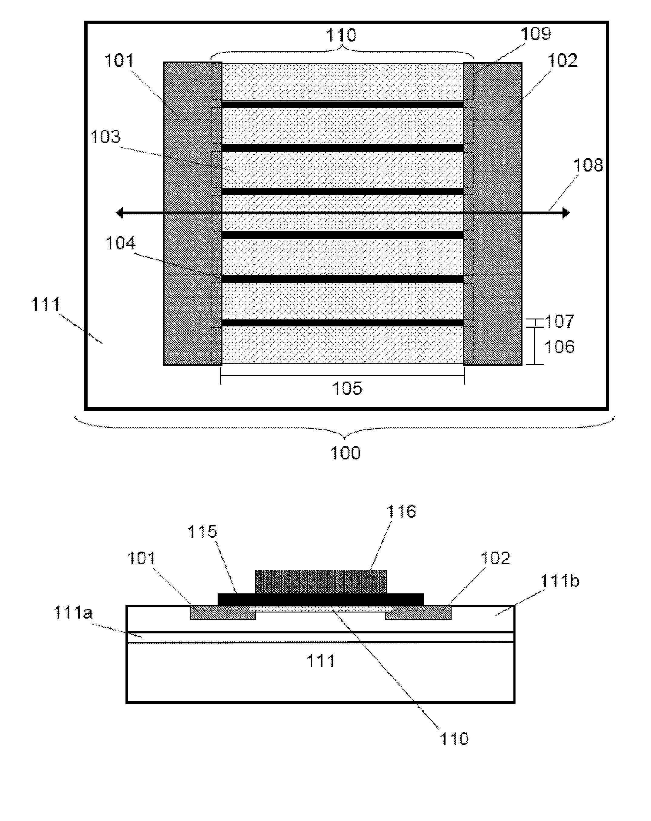
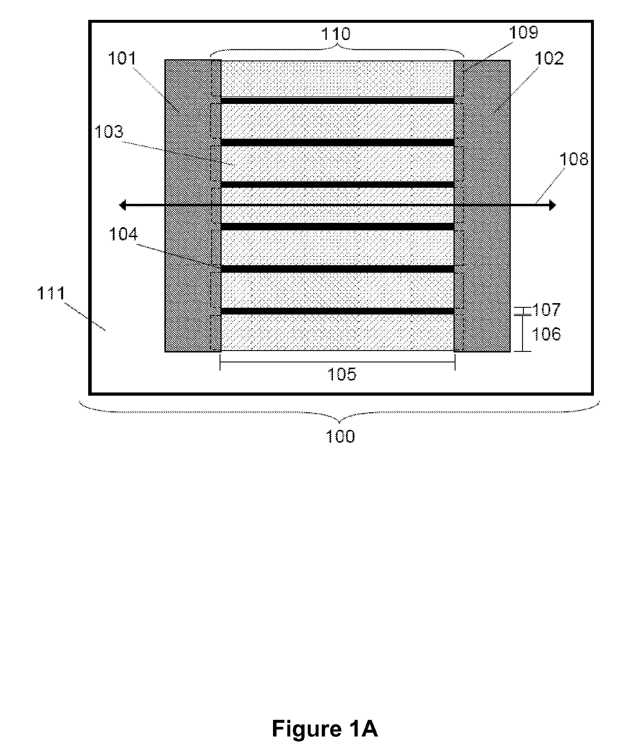
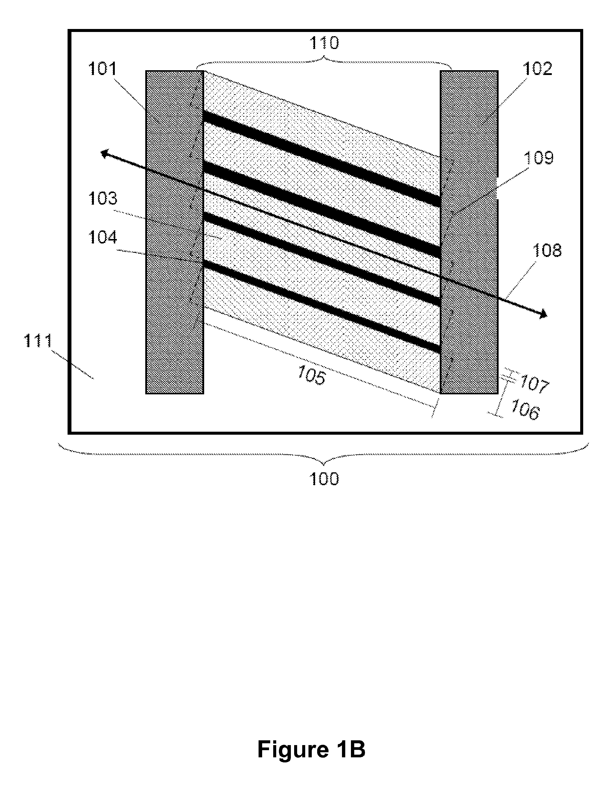
[0174]A new technique to reduce the influence of metallic carbon nanotubes (CNTs)—relevant for large-scale integrated circuits based on CNT-nanonet transistors—is described and verified. Historically, electrical and chemical filtering of the metallic CNTs have been used to improve the ON / OFF ratio of CNT-nanonet transistors; however, the corresponding degradation in ON-current has made these techniques somewhat unsatisfactory. Here, we diverge significantly from the classical approaches in favor of a new approach based on relocation of asymmetric percolation threshold of CNT-nanonet transistors by a technique called “striping”; this allows fabrication of transistors with ON / OFF ratio >1000 and ON-current degradation no more than a factor of 2. We offer first principle numerical models, experimental confirmation, and renormalization arguments to provide a broad theoretical and e...


PUM

PropertyMeasurementUnit
thicknessaaaaaaaaaa
average distanceaaaaaaaaaa
aspect ratioaaaaaaaaaa

Abstract

The present invention provides device components geometries and fabrication strategies for enhancing the electronic performance of electronic devices based on thin films of randomly oriented or partially aligned semiconducting nanotubes. In certain aspects, devices and methods of the present invention incorporate a patterned layer of randomly oriented or partially aligned carbon nanotubes, such as one or more interconnected SWNT networks, providing a semiconductor channel exhibiting improved electronic properties relative to conventional nanotubes-based electronic systems.

Description

CROSS-REFERENCE TO RELATED APPLICATIONS[0001]This application claims the benefit of priority to U.S. provisional Patent Applications 61 / 061,710 filed Jun. 16, 2008 and 61 / 074,254 filed Jun. 20, 2008, which are hereby incorporated by reference in their entirety.STATEMENT REGARDING FEDERALLY SPONSORED RESEARCH OR DEVELOPMENT[0002]This invention was made with government support awarded by the following agencies: National Science Foundation Grant NIRT-0403489 and U.S. Department of Energy Grant DE-FG02-07ER46471. The United States government has certain rights in the invention.BACKGROUND OF INVENTION[0003]Since their discovery in the early 1990s, a great deal has been learned about the composition and properties of carbon nanotube materials. This research has demonstrated that carbon nanotubes exhibit extraordinary mechanical, electronic and chemical properties, which has stimulated substantial interest in developing applied technologies exploiting these properties. Accordingly, substan...

Claims


Application Information

Patent Timeline
Patent Type & Authority Patents(United States)
IPC IPC(8): H01L51/05B82Y10/00H01L51/00
CPCH01L51/0005B82Y10/00H01L51/0014H01L51/0048H01L51/0541H01L51/0545Y10S977/742Y10S977/938H10K71/135H10K71/20H10K85/221H10K10/464H10K10/466
Inventor ROGERS, JOHN A.CAO, QINGALAM, MUHAMMADPIMPARKAR, NINAD
Owner PURDUE RES FOUND INC
Why Eureka
Try Eureka