Differential negative impedance converters and inverters with variable or tunable conversion ratios

a converter and negative impedance technology, applied in the field ofdifferential circuit topology, can solve the problems of limited bandwidth of two applications, small stability margin, and few successful attempts to realize the effect of improving the performance of the system, and achieve the effect of reducing parasitics and good device matching

Active Publication Date: 2015-03-24
HRL LAB
View PDF33 Cites 15 Cited by
  • Summary
  • Abstract
  • Description
  • Claims
  • Application Information

AI Technical Summary

Benefits of technology

[0012]The circuit disclosed herein has the following advantages: The differential topology allows the separation of the bias network from the RF stability analysis; the tunability allows the circuit to be brought near the point of instability without actually going unstable, in addition to being able to tune out parasitics; and the circuit may be implemented in an IC. The IC implementation has further advantages: reduced parasitics due to the small size, plentiful options to implement the bias network, good device matching for the differential topology, the small size permits the circuit to be placed in small gaps, and hundreds or more circuits may be realized for array applications (which would not be practical with the state of the art).

Problems solved by technology

It is well known that these two applications suffer from limited bandwidth, especially as attempts are made to miniaturize them and use, for example, Electrically Small Antennas (ESAs).
However, few attempts to realize this improvement have been successful because first, these circuits are potentially unstable, and second, they must be operated with small stability margin.

Method used


Image

  • Differential negative impedance converters and inverters with variable or tunable conversion ratios
  • Differential negative impedance converters and inverters with variable or tunable conversion ratios
  • Differential negative impedance converters and inverters with variable or tunable conversion ratios

Examples


Embodiment Construction

[0017]A differential circuit topology can produce a tunable floating negative inductance, negative capacitance, negative resistance / conductance, or a combination of the three. Circuits which generate negative capacitance, inductance and / or resistance are commonly referred to as “non-Foster circuits” because they violate Foster's reactance theorem for passive lossless 1-port circuits, which says that the reactance and susceptance must increase with frequency.

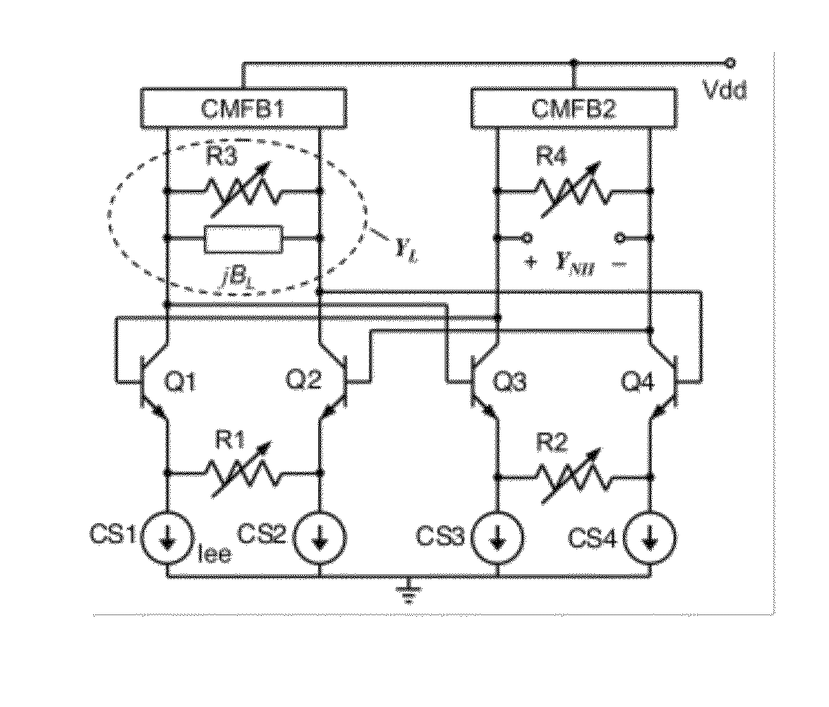
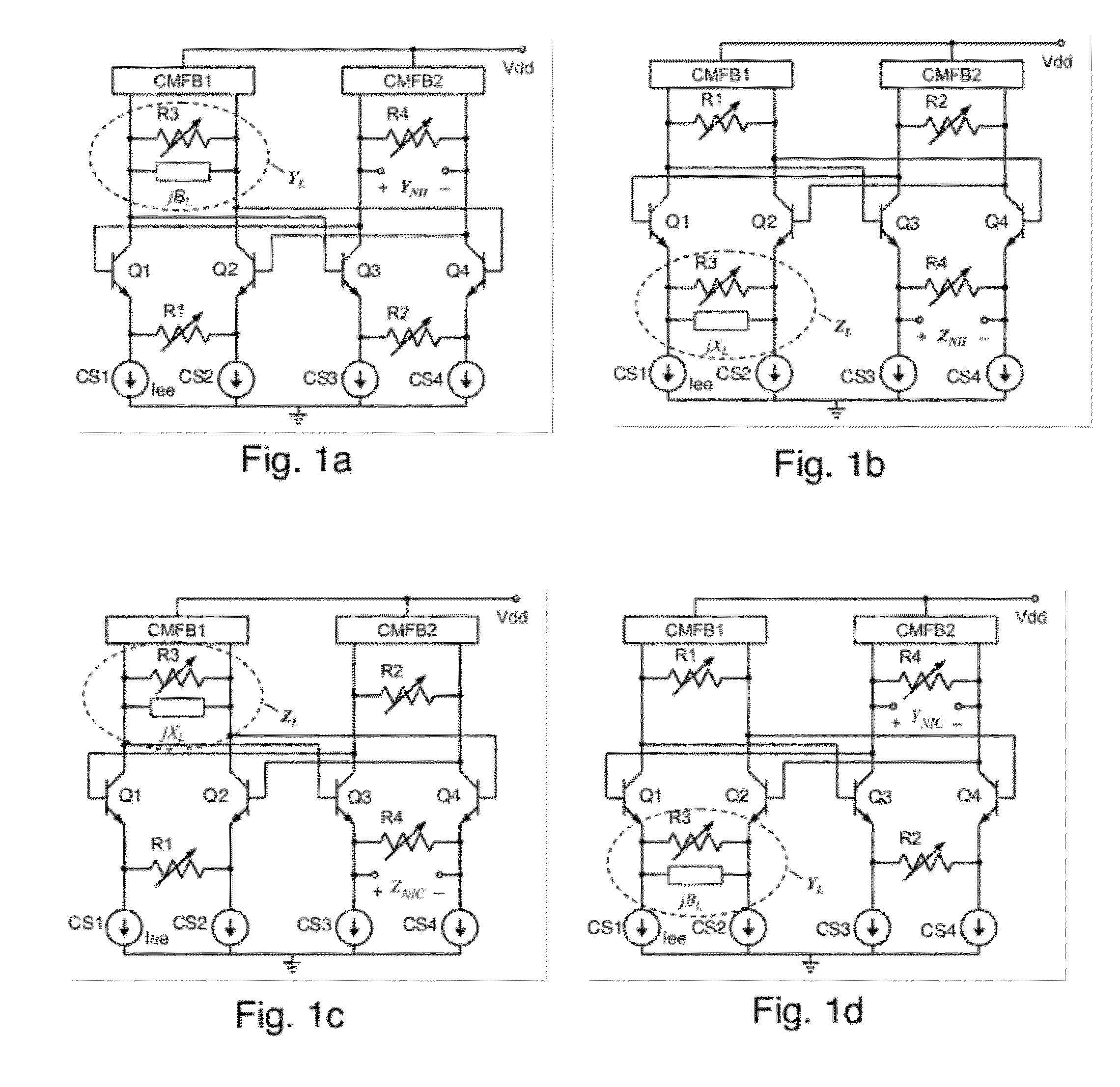
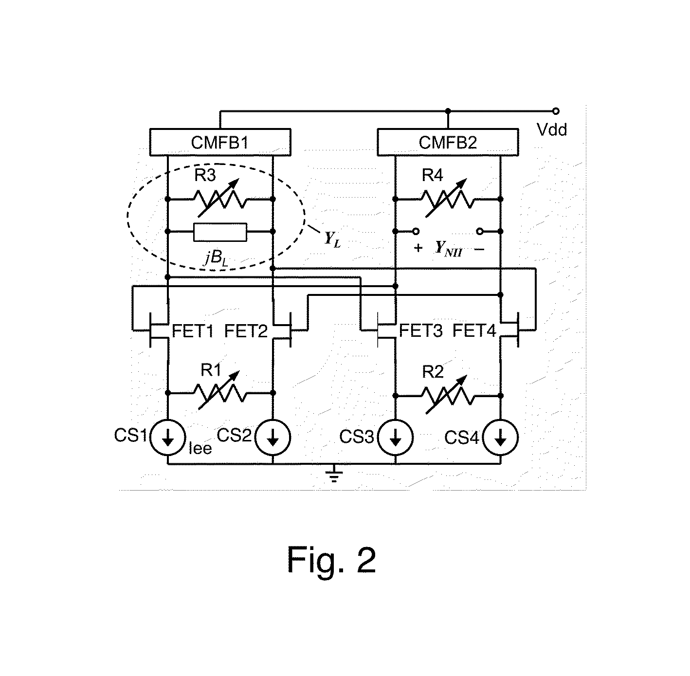
[0018]The circuits is shown in FIGS. 1a-1d each comprises two differential pairs of transistors (Q1, Q2 and Q3, Q4; bipolar transistors are shown, but FETs may be used instead if desired) that are cross-coupled, a load immittance (YL or ZL) connected across one differential pair, four current sources (CS1-CS4), two Common-Mode FeedBack networks (CMFB1 and CMFB2), four tunable (variable) resistors (R1-R4) connected across the differential pairs, and two terminals across which the desired immittance is present (VNII in FIGS. 1a and...


PUM


Abstract

A differential circuit topology that produces a tunable floating negative inductance, negative capacitance, negative resistance / conductance, or a combination of the three. These circuits are commonly referred to as “non-Foster circuits.” The disclosed embodiments of the circuits comprises two differential pairs of transistors that are cross-coupled, a load immittance, multiple current sources, two Common-Mode FeedBack (CMFB) networks, at least one tunable (variable) resistance, and two terminals across which the desired immittance is present. The disclosed embodiments of the circuits may be configured as either a Negative Impedance Inverter (NII) or a Negative Impedance Converter (NIC) and as either Open-Circuit-Stable (OCS) and Short-Circuit-Stable (SCS).

Description

CROSS REFERENCE TO RELATED APPLICATIONS[0001]This application claims the benefit of U.S. Provisional Application Ser. No. 61 / 473,076 filed on Apr. 7, 2011 and entitled “Wideband Adaptable Artificial Impedance Surface”, the disclosure of which is hereby incorporated herein by reference.[0002]This application also claims the benefit of U.S. Provisional Application Ser. No. 61 / 505,037 filed on Jul. 6, 2011 and entitled “Differential Negative Impedance Converters and Inverters with Tunable Conversion Ratios”, the disclosure of which is hereby incorporated herein by reference.[0003]This application is related to U.S. patent application Ser. No. 13 / 177,479 filed on Jul. 6, 2011 and entitled “Wide Bandwidth Automatic Tuning Circuit”, the disclosure of which is hereby incorporated hereby by reference.TECHNICAL FIELD[0004]The present invention is directed to a differential circuit topology that produces a tunable or variable negative inductance, negative capacitance, negative resistance / cond...

Claims


Application Information

Patent Timeline
Patent Type & Authority Patents(United States)
IPC IPC(8): H03H11/10H03H11/48
CPCH03H11/10H03H11/48H03F1/56H03F2200/369H04B1/0458H04B1/18H03H11/44
Inventor HITKO, DONALD A.WHITE, CARSON R.YUNG, MICHAEL W.MATTHEWS, DAVID S.MORTON, SUSAN L.MAY, JASON W.COLBURN, JOSEPH S.
Owner HRL LAB
Why Eureka
Try Eureka