
Wafer process body, wafer processing member, wafer processing temporary adhesive material, and method for manufacturing thin wafer

a technology of temporary adhesive and wafer, which is applied in the direction of film/foil adhesives without carriers, film/foil adhesives, transportation and packaging, etc. it can solve the problems of deformation of resin and fouling of equipment during processing, the adhesion between the supporting body and the wafer is so strong and hard, and the removal is difficult. , to achieve the effect of high heat resistance, easy breakage, and easy detachment from the supporting body

Active Publication Date: 2015-04-07
SHIN ETSU CHEM IND CO LTD
View PDF13 Cites 7 Cited by
  • Summary
  • Abstract
  • Description
  • Claims
  • Application Information

AI Technical Summary

Benefits of technology

The present invention provides a method for manufacturing a thin wafer with high productivity using a temporary adhesive material. The temporary adhesive layer is easy to apply, can be used in a wide range of semiconductor film formation processes, and can form a uniform film thickness on a non-planar wafer. The thin wafer obtained can be easily detached from the supporting body at room temperature, making it breakable. The technical effects of the invention are simplifying the temporary adhesion process of a wafer with a supporting body, improving the uniformity of the process, and making it easier to manufacture thin wafers.

Problems solved by technology

However, in the former method, the thermoplastic resin is of a low elastic modulus and flowable at normal temperature, so that, depending on composition of the stacked substrate, there is a risk of causing deformation of the resin and fouling of an equipment during processing.
In the latter method, it can be suitably used in the horizontal sliding method wherein heating is done for removal; but in the method wherein one surface of the stacked substrate is fixed horizontally while the other surface is pulled up with a certain angle from the horizontal direction, adhesion with the supporting body and the wafer is so strong and hard that removal is difficult; and thus, this poses a problem that its application to the actual manufacturing process is difficult.

Method used


Image

  • Wafer process body, wafer processing member, wafer processing temporary adhesive material, and method for manufacturing thin wafer
  • Wafer process body, wafer processing member, wafer processing temporary adhesive material, and method for manufacturing thin wafer
  • Wafer process body, wafer processing member, wafer processing temporary adhesive material, and method for manufacturing thin wafer

Examples


synthesis example 1

[0173]Into a 1-L flask equipped with a stirrer, a cooling equipment, and a thermometer were taken 234 g (13 moles) of water and 35 g of toluene; and then, they were heated at 80° C. in an oil bath. Into a dropping funnel were taken 183.6 g (0.8 mole) of norbornyl trichloro silane, 12.9 g (0.1 mole) of dimethyl dichloro silane, and 10.9 g (0.1 mole) of trimethyl chloro silane; and then, this mixture was gradually added into the flask in one hour with stirring. After completion of the addition, heating was further continued for aging at 80° C. for one hour. The resulting mixture was cooled statically to room temperature, and then, the separated aqueous layer was removed. After the organic layer was mixed with a 10% aqueous solution of sodium sulfate with stirring for 10 minutes, this mixture was allowed to stand for 30 minutes, and then, the separated aqueous layer was removed. This washing operation by water to remove the separated aqueous layer was repeated until the toluene layer b...

synthesis example 2

[0175]Similarly to Synthesis Example 1, 234 g (13 moles) of water and 35 g of toluene were taken into a 1-L flask; and then, they were heated at 80° C. in an oil bath. The subsequent procedures were followed similarly to Synthesis Example 1 except that 206.6 g (0.9 mole) of norbornyl trichloro silane, 7.1 g (0.05 mole) of methyl vinyl dichloro silane, and 5.4 g (0.05 mole) of trimethyl chloro silane were taken into a dropping funnel; and as a result, 140 g of a solid organopolysiloxane (Resin 2) was obtained.

[0176]The obtained organopolysiloxane contained 90 mol % of the T Unit, 5 mol % of the D unit, and 5 mol % of the M Unit. In addition, 0.1 mole of the terminal silanol group and 0.034 mole of the terminal vinyl group per 100 g of the organopolysiloxane. The appearance thereof was a colorless and transparent solid with the weight-average molecular weight of 5,900. Contents of the norbornyl group and the vinyl group, relative to totality of the organic groups and the hydrogen atom...

synthesis example 3

[0177]As the alkenyl-containing oreganopolysiloxane (A1), 100 g of the solid organopolysiloxane (Resin 2) obtained by Synthesis Example 2 was dissolved into 100 g of toluene to obtain a solution with the solid concentration thereof being 50%. Into this solution was added a platinum catalyst with the amount thereof being 20 ppm as the platinum atom relative to the resin; and then, 27.5 g of the compound (SiH equivalent of 1473 g / mol) shown by the following formula (9) as the hydrosilyl-containing compound (A2) was gradually added thereinto at 60° C. At this time, heat generation due to the reaction was recognized. This amount corresponds to 0.55 of the H / Vi ratio (ratio of the SiH group to totality of the alkenyl group). The reaction was carried out at 100° C. for two hours to complete the reaction. Thereafter, toluene was removed by vacuum distillation to obtain a solidified reaction product, which was then redissolved into isododecane. The resulting solution was filtrated through a...


PUM

PropertyMeasurementUnit
mol %aaaaaaaaaa
mol %aaaaaaaaaa
temperatureaaaaaaaaaa

Abstract

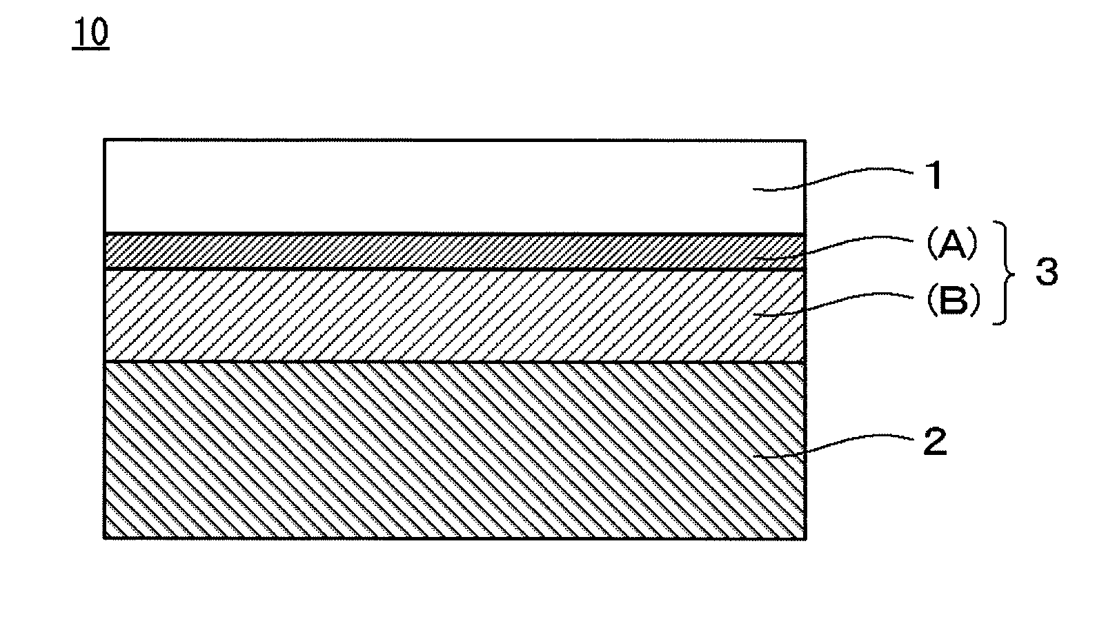
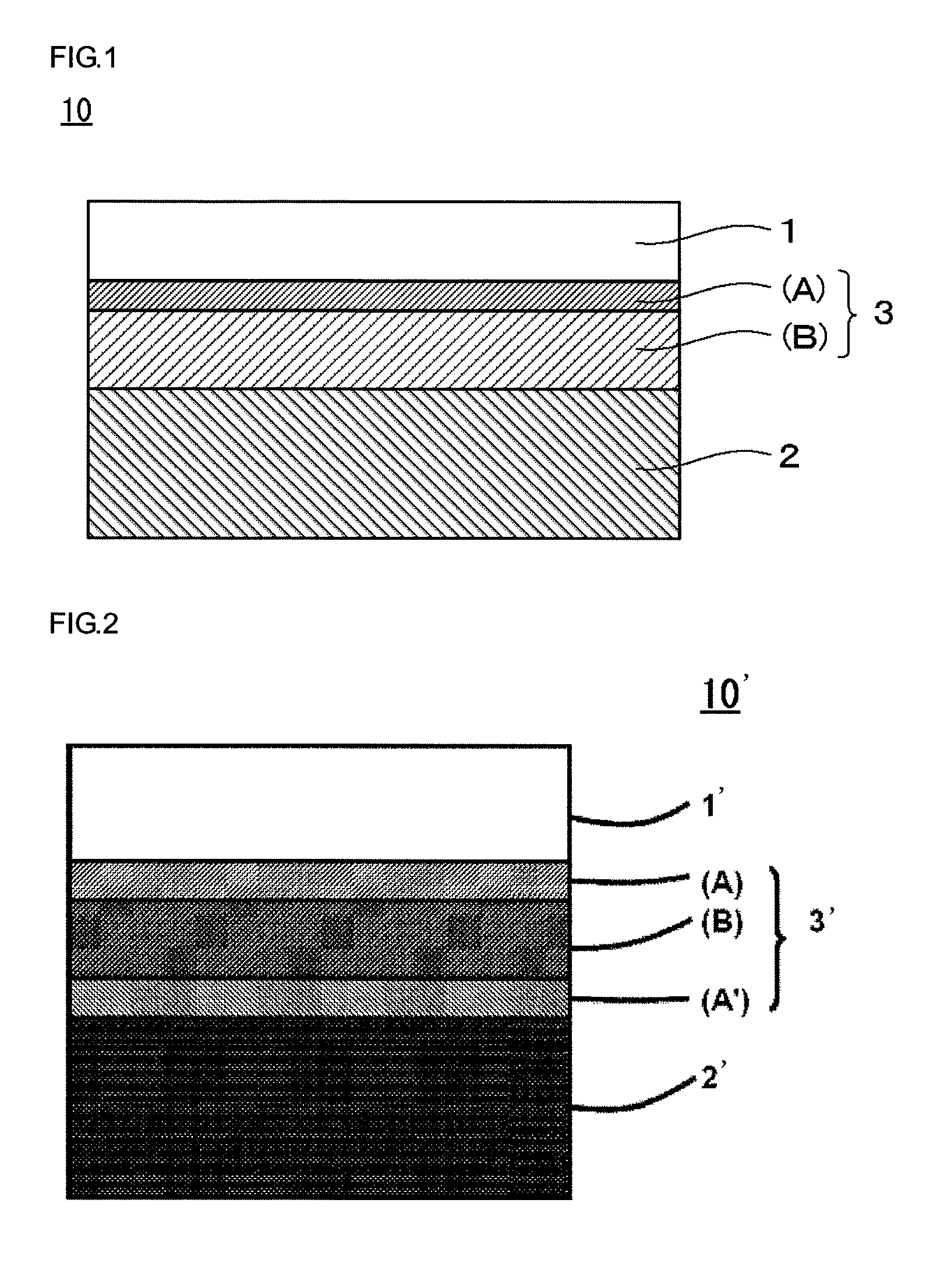
Disclosed is a wafer process body, a temporary adhesive layer is formed on a supporting body, and a wafer having a circuit-formed front surface and a to-be-processed back surface is stacked on the temporary adhesive layer, wherein the temporary adhesive layer is provided with a first temporary adhesive layer including a non-aromatic saturated hydrocarbon group-containing organopolysiloxane layer (A) which is adhered to the front surface of the wafer so as to be detachable and a second temporary adhesive layer comprised of a thermosetting-modified siloxane polymer layer (B) which is stacked on the first temporary adhesive layer and adhered to the supporting body so as to be detachable. Thus, temporary adhesion of a wafer with a supporting body may become easy, process conformity with the TSV formation process and with the wafer-back surface-wiring process may become high, and removal may be done easily, with high productivity.

Description

BACKGROUND OF THE INVENTION[0001]1. Field of the Invention[0002]The present invention relates to a wafer process body, a wafer processing member, and a wafer processing temporary adhesive material, which is capable of giving a thin wafer effectively, respectively, and a method for manufacturing a thin wafer.[0003]2. Description of the Related Art[0004]A three-dimensional semiconductor mount becomes indispensable to realize higher density, larger capacity, higher processing speed, and lower power consumption than ever. According to the three-dimensional semiconductor mounting technology, a semiconductor chip is made thin, and then this is stacked in multilayer while connecting them by a silicon through electrode (TSV: through silicon via). To realize this, a process to make a substrate formed with a semiconductor circuit thin by grinding a surface not formed with a circuit (also referred to as the “back surface”) and a process to form an electrode including TSV on the back surface th...

Claims


Application Information

Patent Timeline
Patent Type & Authority Patents(United States)
IPC IPC(8): H01L21/00C09J7/10H01L21/304H01L21/683
CPCC09J7/00H01L21/304H01L21/6835C09J7/0239H01L2221/68327H01L2221/6834H01L2221/68381C09J2201/122C09J2201/36C09J2203/326C09J2483/00C09J7/22C09J7/30Y10T428/2852C09J7/10C09J2301/208C09J2301/122H01L21/02304
Inventor TAGAMI, SHOHEISUGO, MICHIHIROYASUDA, HIROYUKIFURUYA, MASAHIROKATO, HIDETO
Owner SHIN ETSU CHEM IND CO LTD
Learn More