Semiconductor device and driving method thereof

a technology of semiconductor devices and driving methods, applied in semiconductor devices, digital storage, instruments, etc., can solve problems such as significant problems, deterioration of transistors, and large power consumption, and achieve the effects of suppressing oxide semiconductor carrier generation, reducing impurities and oxygen vacancy, and reducing oxygen vacancy

Active Publication Date: 2015-04-07
SEMICON ENERGY LAB CO LTD
View PDF134 Cites 12 Cited by
  • Summary
  • Abstract
  • Description
  • Claims
  • Application Information

AI Technical Summary

Benefits of technology

[0009]Thus, an object is to provide a semiconductor memory device with low power consumption in which the frequency of refresh operation for holding data is decreased.
[0029]Further, it is not necessary to provide a counter which counts timing of the refresh operation for a long time as a refresh timing detection circuit, whereby a semiconductor memory device including a refresh timing detection circuit having a small area and low power consumption can be obtained.

Problems solved by technology

A conventional DRAM needs to perform a refresh operation at an interval of several tens of milliseconds to hold data, which results in large power consumption.
In addition, a transistor therein is frequently turned on and off; thus, deterioration of the transistor is a problem.
These problems become significant as the memory capacity increases and transistor miniaturization advances.

Method used


Image

  • Semiconductor device and driving method thereof
  • Semiconductor device and driving method thereof
  • Semiconductor device and driving method thereof

Examples


embodiment 1

[0059]In this embodiment, a semiconductor memory device according to one embodiment of the present invention will be described.

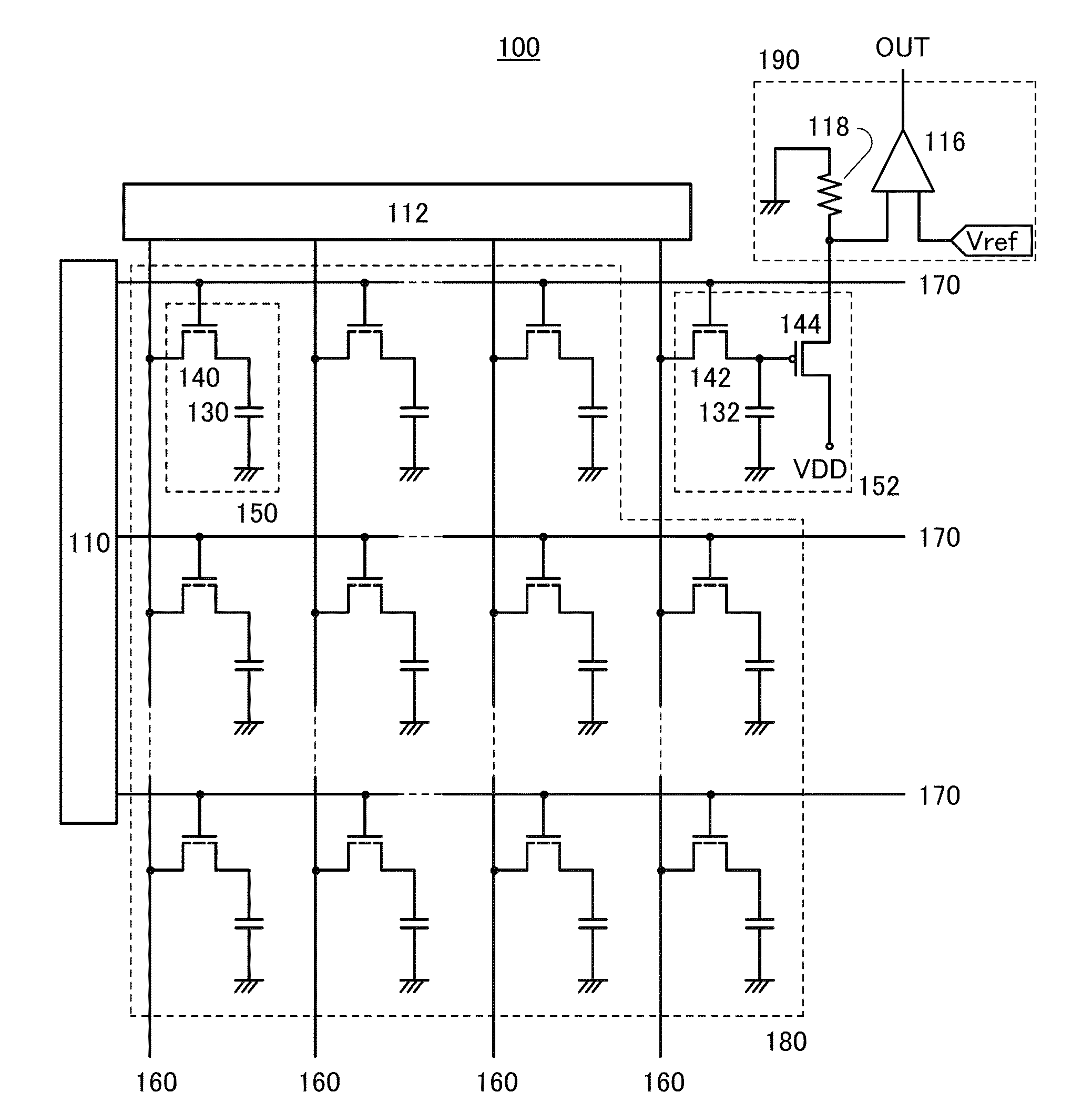
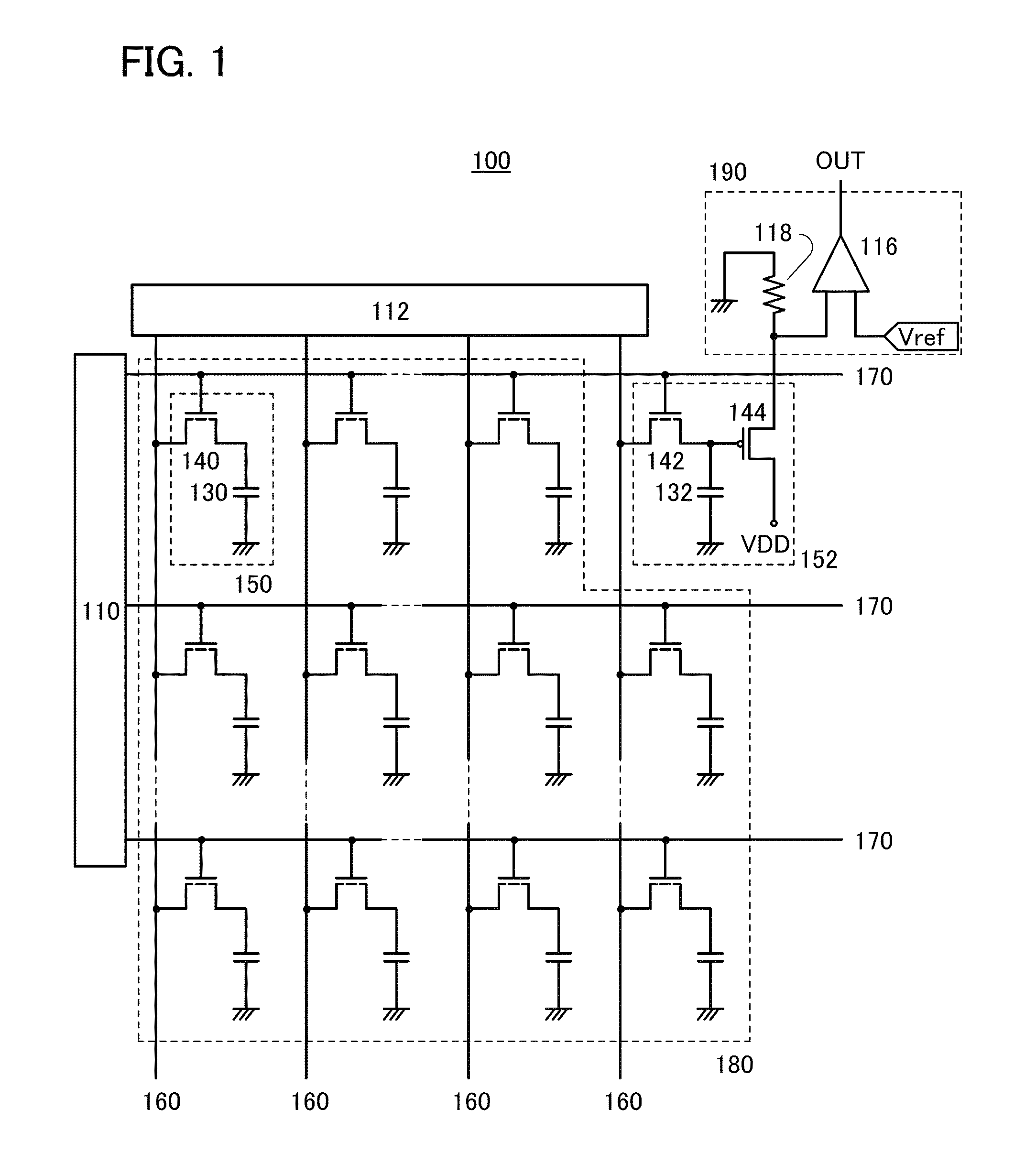
[0060]FIG. 1 is a circuit diagram of a memory module 100 which is a semiconductor memory device.

[0061]The memory module 100 includes a memory cell array 180 including a plurality of memory cells 150 arranged in matrix, a refresh timing detection circuit including a reference cell 152 and a comparison circuit 190, a row decoder 110, a column decoder 112, bit lines 160, and word lines 170.

[0062]The memory cell 150 includes a first transistor 140 using an oxide semiconductor and a first capacitor 130. With the use of an oxide semiconductor, the off-state current of the first transistor 140 can be reduced.

[0063]In this specification, in order to distinguish a transistor formed using an oxide semiconductor from the other transistors, a signal shown as the first transistor 140 in FIG. 1 and the like is used as a transistor using an oxide semiconductor.

[0064]The re...

embodiment 2

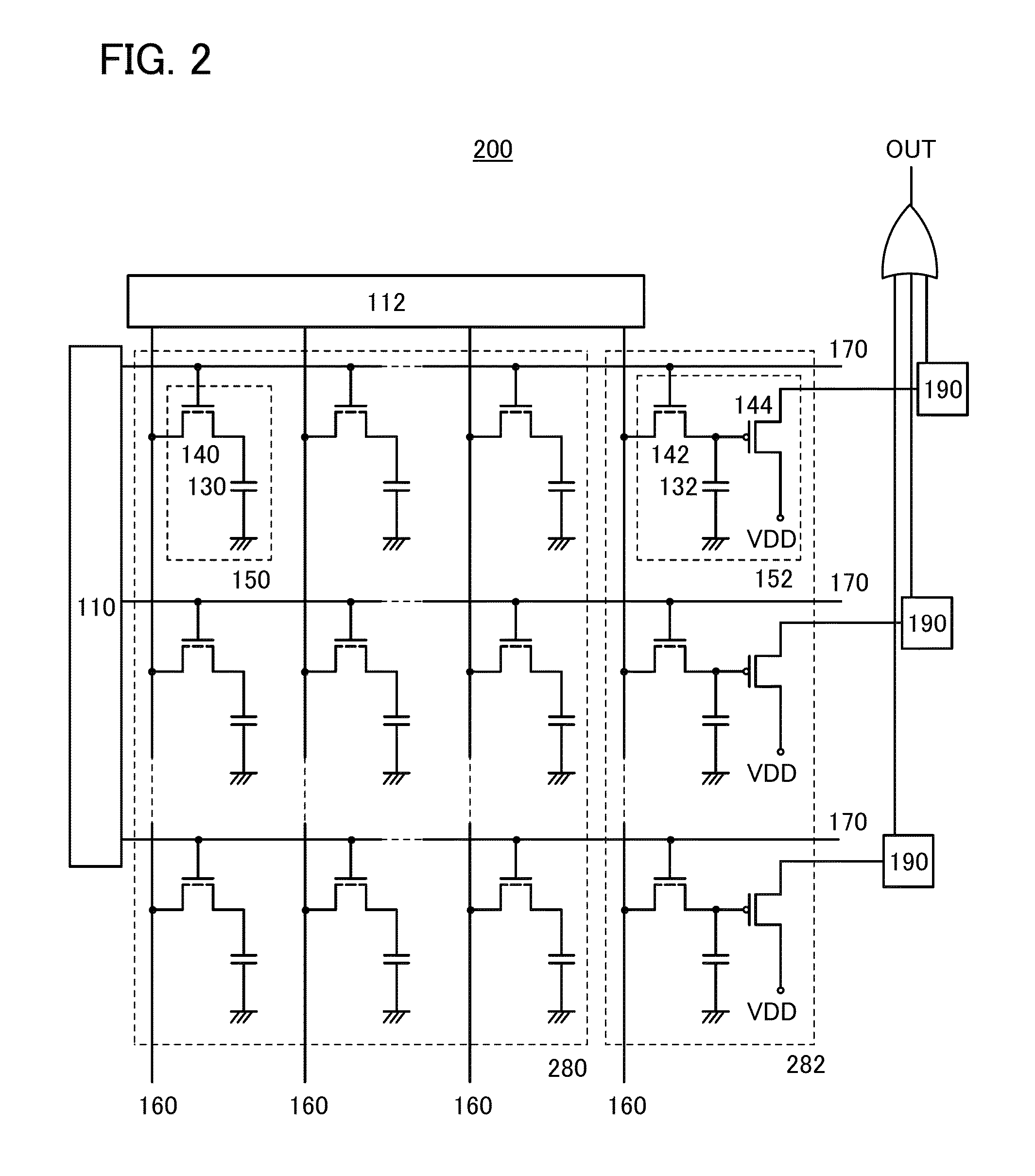
[0223]In this embodiment, a memory module 200 which has a different structure from that of the memory module 100 described in Embodiment 1 will be described with reference to FIG. 2.

[0224]The memory module 200 is different from the memory module 100 in that it includes a reference cell group 282 including a plurality of reference cells 152.

[0225]Further, since the plurality of reference cells 152 is included, a memory cell array 280 has a storage capacity little smaller than that of the memory cell array 180.

[0226]Each of the plurality of reference cells 152 included in the reference cell group 282 may be connected to the bit line 160 in the same column, but the present invention is not limited thereto. For example, the different reference cells 152 may be connected to the bit lines 160 in different columns. Further, the reference cells 152 are not necessarily close to each other.

[0227]In the reference cell group 282, when the drain current flows from each of the reference cells 152...

embodiment 3

[0230]In this embodiment, a memory module 300 having a structure different from those of the memory module 100 and the memory module 200 described in Embodiment 1 and Embodiment 2 will be described with reference to FIG. 3.

[0231]The memory module 300 is different from the memory module 100 and the memory module 200 in that the third transistor 144 is not included in a reference cell 352 corresponding to the reference cell 152.

[0232]Therefore, in the comparator 116, Vref and the potential of the second capacitor 132 are compared. That is, when the potential of the second capacitor 132 is gradually decreased and becomes lower than Vref, the refresh operation may be performed to the memory cell array 180 and the reference cell 352.

[0233]This embodiment has a structure in which the third transistor 144 is not provided, whereby the structure is simplified for easy manufacture.

[0234]On the other hand, in order to detect the timing of the refresh operation accurately, the capacitance of th...


PUM


Abstract

In a memory module including a memory cell array including memory cells arranged in matrix, each including a first transistor using an oxide semiconductor and a first capacitor; a reference cell including a p-channel third transistor, a second capacitor, and a second transistor using an oxide semiconductor; and a refresh timing detection circuit including a resistor and a comparator, wherein when a potential is supplied to the first capacitor through the first transistor, a potential is supplied to the second capacitor through the second transistor, wherein a drain current value of the third transistor is changed in accordance with the potential stored in the second capacitor, and wherein when the drain current value of the third transistor is higher than a given value, a refresh operation of the memory cell array and the reference cell are performed.

Description

BACKGROUND OF THE INVENTION[0001]1. Field of the Invention[0002]The present invention relates to a semiconductor memory device which includes a circuit including a semiconductor element such as a transistor, and a driving method thereof.[0003]2. Description of the Related Art[0004]A dynamic random access memory (DRAM) is a semiconductor memory device where one bit of data can be stored with use of one transistor and one capacitor. The DRAM has advantages such as a small area per unit memory cell, easiness in integration for modularization, and low manufacturing cost.[0005]The DRAM requires an operation of recharge (refresh) before necessary electric charge is lost. A counter of a memory controller or a microcomputer incorporating a memory controller counts timing for performing a refresh operation, and the refresh operation is performed when the count becomes a predetermined value.[0006]Since frequent refresh operations increase power consumption, reduction of the frequency of the r...

Claims


Application Information

Patent Timeline
Patent Type & Authority Patents(United States)
IPC IPC(8): G11C11/24G11C11/401G11C11/404G11C11/4099H01L27/108H01L27/12
CPCG11C11/404G11C11/401G11C11/4099H01L27/10897H01L27/1218H01L27/1225H01L27/10873H10B12/05H10B12/50G11C11/406H10B12/30G11C5/10G11C11/4091
Inventor ATSUMI, TOMOAKITAKEWAKI, YOSHIYA
Owner SEMICON ENERGY LAB CO LTD
Why Eureka
Try Eureka