

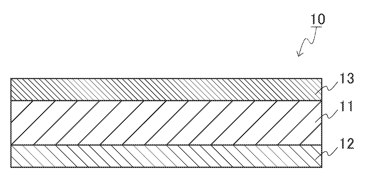
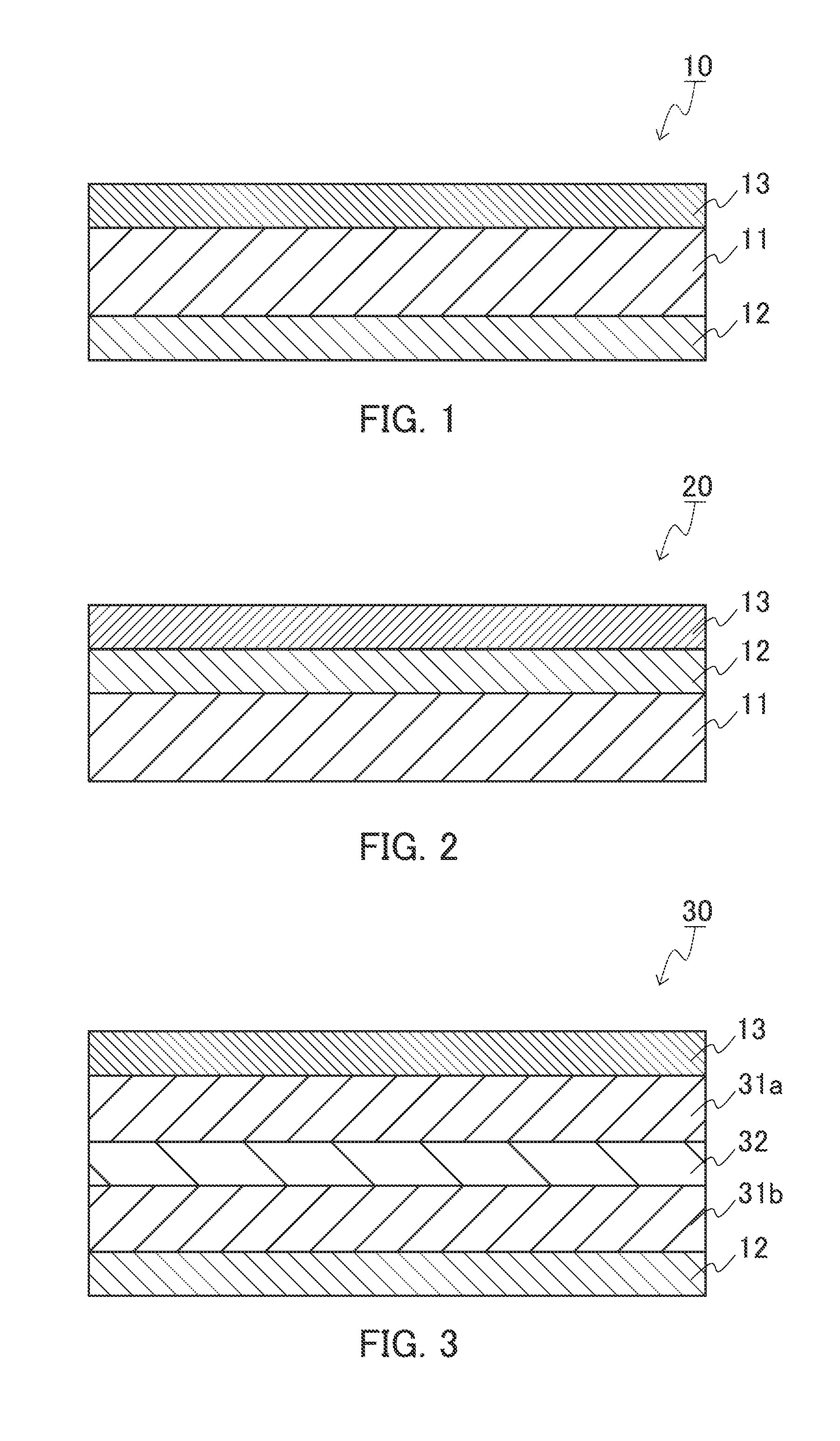
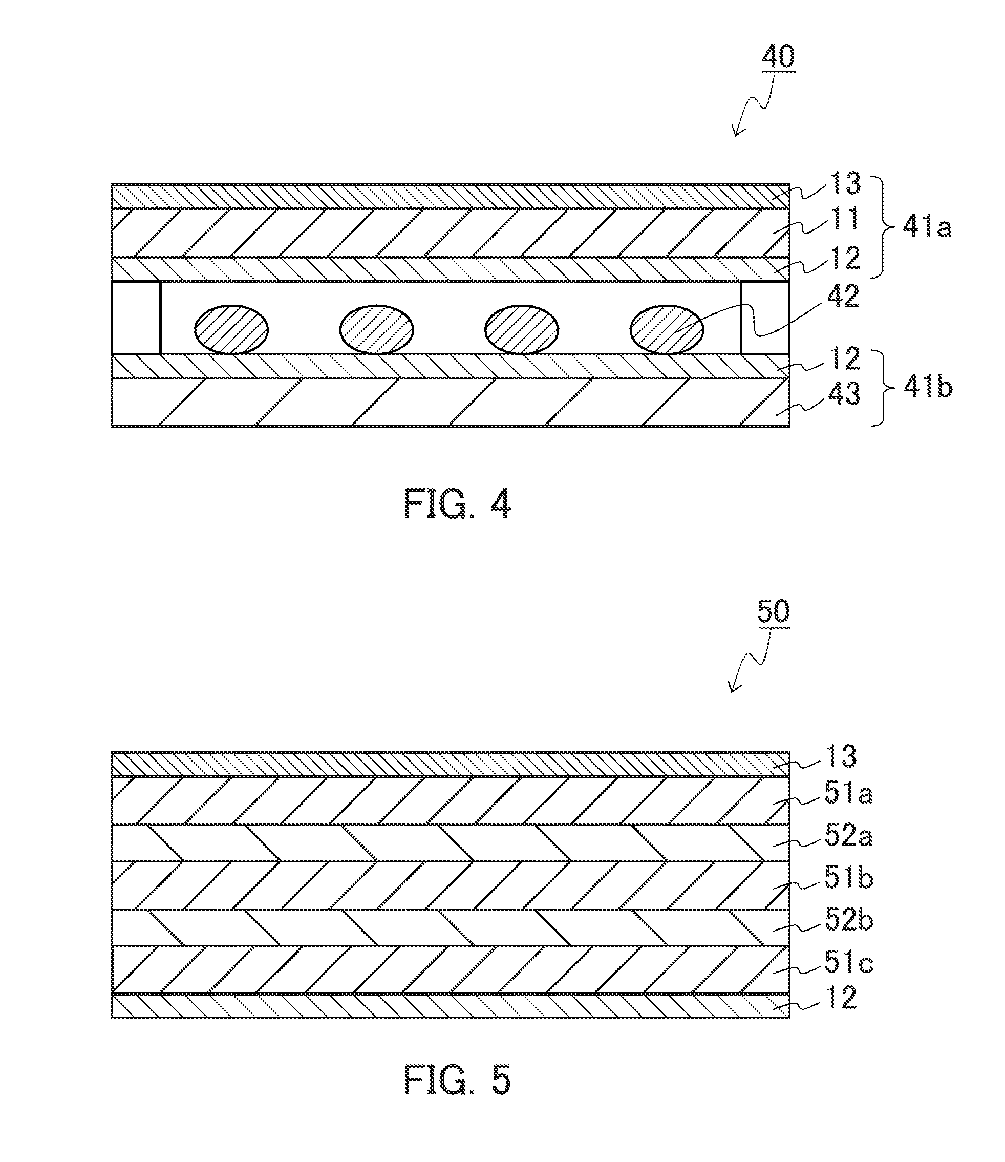
Transparent conductive film, electronic device, and touch panel
a technology of transparent conductive film and electronic devices, applied in the direction of conductive layers on insulating supports, instruments, transportation and packaging, etc., can solve the problems of inability to use conductive glass depending on flexibility and processability, and achieve superior soil resistance, superior hardness, and superior abrasion resistance.
- Summary
- Abstract
- Description
- Claims
- Application Information
AI Technical Summary
Benefits of technology
Problems solved by technology
Method used
Image

Examples
example 1
[0124]
[0125]A resin raw material containing the component (A) (“OPSTAR Z7540” (trade name) produced by JSR Corporation; solid content: 56 wt %, solvent: butyl acetate / methyl ethyl ketone (MEK)=76 / 24 (weight ratio)) in which nano-silica particles having surfaces modified with organic compounds containing polymerizable unsaturated groups (the component (D)) were dispersed was provided.
[0126]The resin raw material contains dipentaerythritol and isophorone diisocyanate-based polyurethane as the component (A) (ultraviolet-curable compound) and contains silica fine particles having surfaces modified with organic molecules (weight-average particle size: 100 nm or less) as the component (D) at the weight ratio of 2:3 (component (A) in total: component (D)). The refractive index of the cured film of the resin raw material was 1.485.
[0127]Relative to 100 parts by weight (the solid content) of this resin raw material, 0.2 parts by weight of reactive fluorine-containing compound (“OPTOOL® DAC” ...
example 2
[0133]The transparent conductive film of this Example was obtained in the same manner as in Example 1 except that the hard coat layer having a thickness of 15 μm was formed.
example 3
[0134]The transparent conductive film of this Example was obtained in the same manner as in Example 1 except that the amount of the reactive fluorine-containing compound was 0.1 parts by weight and the amount of the reactive silicon-containing compound was 0.5 parts by weight.
PUM
| Property | Measurement | Unit |
|---|---|---|
| weight-average particle size | aaaaa | aaaaa |
| weight-average particle size | aaaaa | aaaaa |
| thickness | aaaaa | aaaaa |
Abstract
Description
Claims
Application Information