

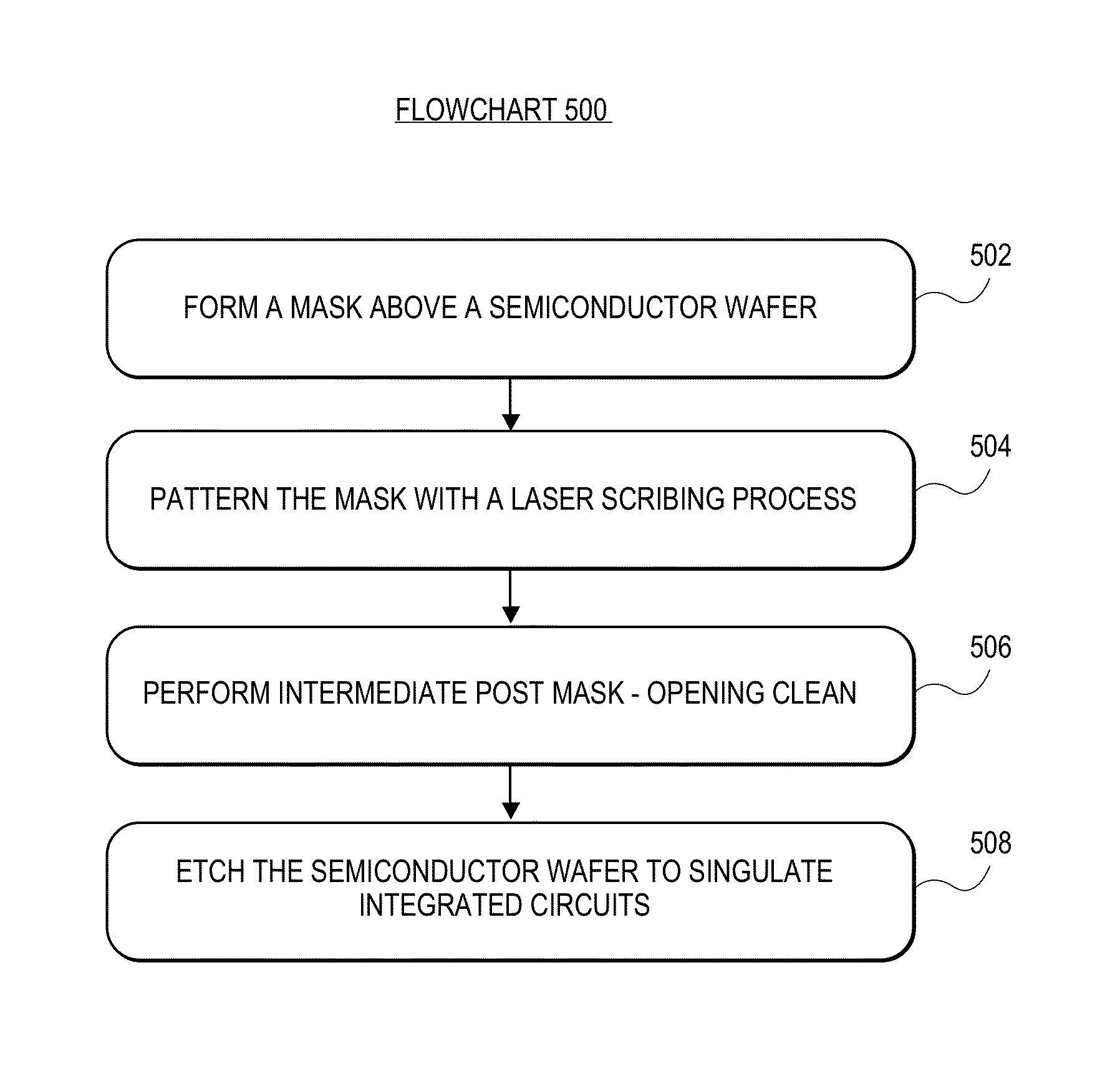
Wafer dicing using hybrid laser scribing and plasma etch approach with intermediate non-reactive post mask-opening clean
a plasma etching and laser scribing technology, applied in the field of semiconductor wafer dicing, can solve the problems of chip and gouge formation along the severed edges of the dice, inoperable integrated circuit, crack formation and propagation,
- Summary
- Abstract
- Description
- Claims
- Application Information
AI Technical Summary
Benefits of technology
Problems solved by technology
Method used
Image

Examples
first embodiment
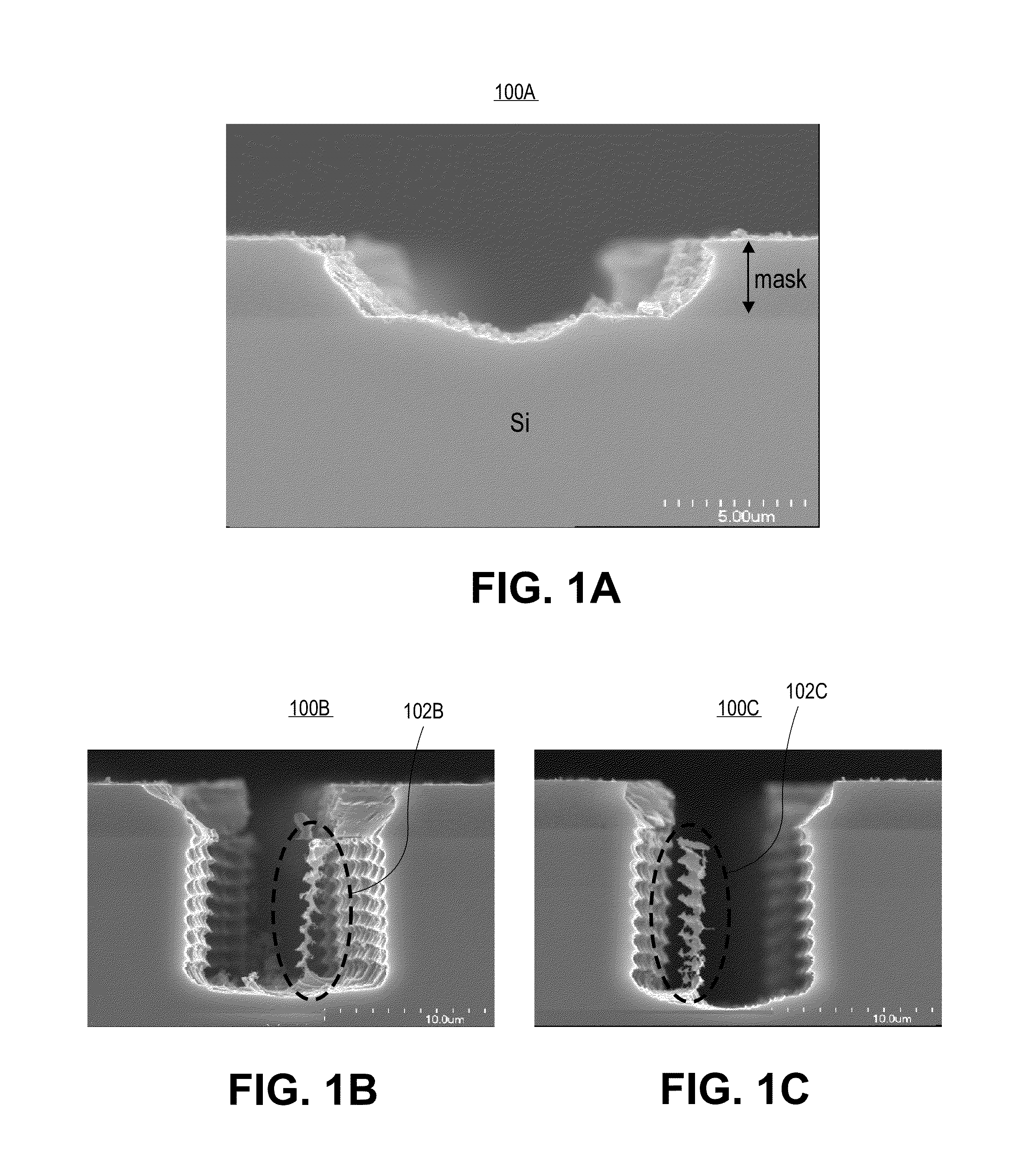
[0074]In accordance with a first embodiment, the plasma-based cleaning process is reactive to exposed regions of the substrate 604 in that the exposed regions are partially etched during the cleaning process. In one such embodiment, Ar or another non-reactive gas (or the mix) is combined with SF6 for a highly-biased plasma treatment for cleaning of scribed openings. The plasma treatment using mixed gases Ar+SF6 under high-bias power is performed for bombarding mask-opened regions to achieve cleaning of the mask-opened regions. In the reactive breakthrough process, both physical bombardment from Ar and SF6 along with chemical etching due to SF6 and F-ions contribute to cleaning of mask-opened regions. The approach may be suitable for photoresist or plasma-deposited Teflon masks 602, where breakthrough treatment leads to fairly uniform mask thickness reduction and a gentle Si etch. Such a breakthrough etch process, however, may not be best suited for water soluble mask materials.
[0075...
second embodiment
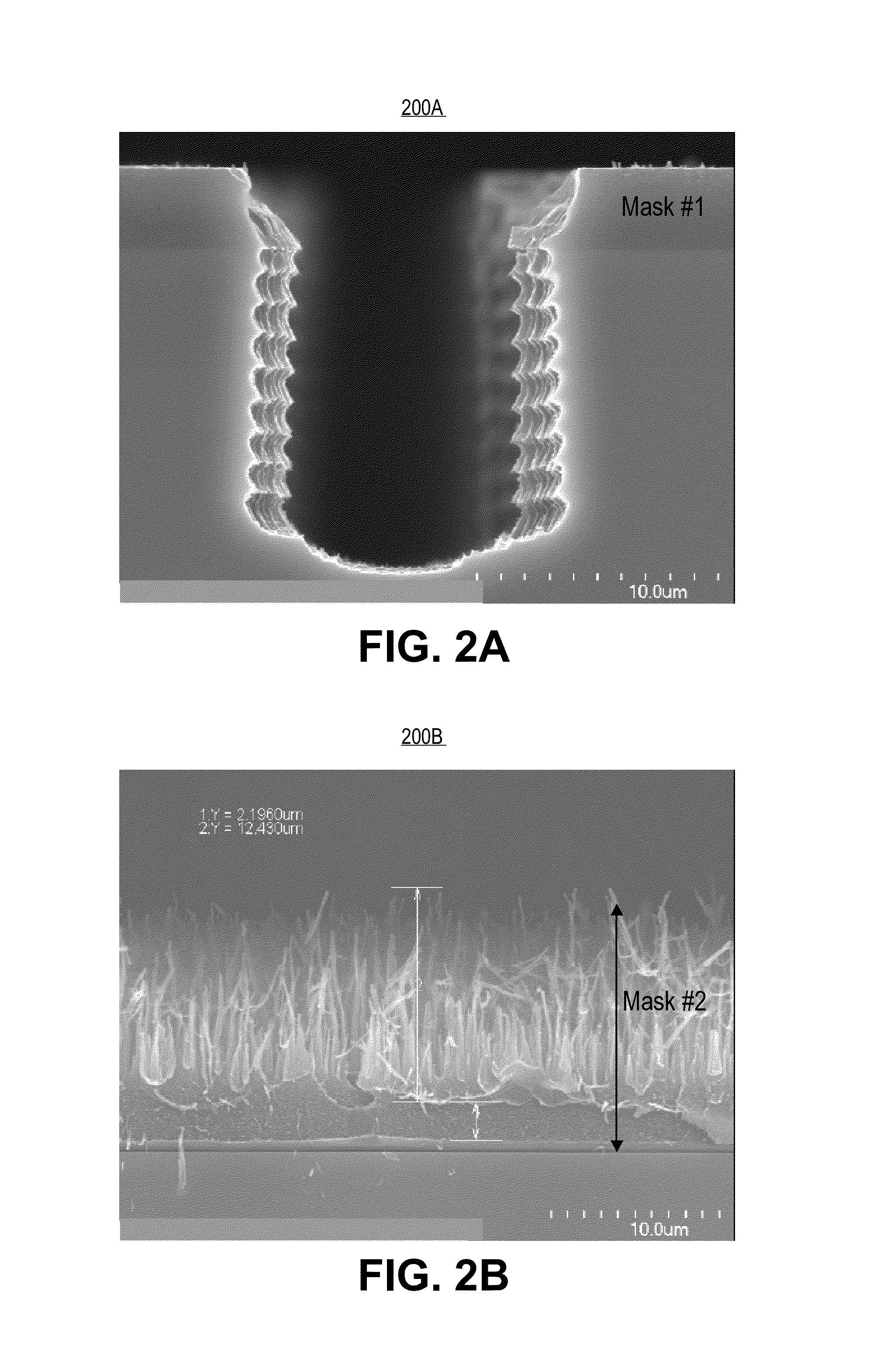
[0076]In accordance with a second embodiment, the plasma-based cleaning process is non-reactive to exposed regions of the substrate 604 in that the exposed regions are not or only negligible etched during the cleaning process. In one such embodiment, only non-reactive gas plasma cleaning is used. For example, Ar or another non-reactive gas (or the mix) is used to perform a highly-biased plasma treatment both for mask condensation and cleaning of scribed openings. In the case of FIGS. 11A-11D, the process would be similar with the exclusion of the change demonstrated in FIG. 11C, since the non-reactive treatment here would not etch the silicon. The approach may be suitable for water-soluble masks or for thinner plasma-deposited Teflon 602. In an exemplary embodiment of the latter case, an SF6+Ar breakthrough cleaning process exhibits an etch rate of approximately 7.66 microns / minute for as-deposited plasma-based Teflon. By contrast, an Ar-only breakthrough cleaning process exhibits a...
PUM
 Abstract
Description
Claims
Application Information