Scanning ion microscope and secondary particle control method

a scanning ion microscope and secondary particle technology, applied in the field of scanning ion microscopes, can solve the problems of specimen image distortion with respect to actual image, inability to completely solve the problem of reducing the electrification of the specimen, and inattention to the existence of electric charge or secondary electrons in the transmitted beam, so as to prevent the distortion of the observation image

Active Publication Date: 2015-06-16
HITACHI HIGH-TECH CORP
View PDF55 Cites 2 Cited by
  • Summary
  • Abstract
  • Description
  • Claims
  • Application Information

AI Technical Summary

Benefits of technology

[0034]According to the present invention, it is possible to observe a specimen minutely and prevent distortion of an observation image even if a specimen containing insulators is charged partially.

Problems solved by technology

In a case where a specimen containing an insulator is observed with a scanning ion microscope, there is an issue that an image of the specimen is distorted with respect to an actual image as a result of the path of the ion beam being locally bent by partial electrification of the specimen.
This cannot be completely solved by reducing electrification on the specimen.
Furthermore, since the conventional thin film utilizing method described in Patent Document 9 does not care about convergence characteristics of the beam, existence of electric charge or secondary electrons in the transmitted beam has not been paid attention.

Method used


Image

  • Scanning ion microscope and secondary particle control method
  • Scanning ion microscope and secondary particle control method
  • Scanning ion microscope and secondary particle control method

Examples


first embodiment

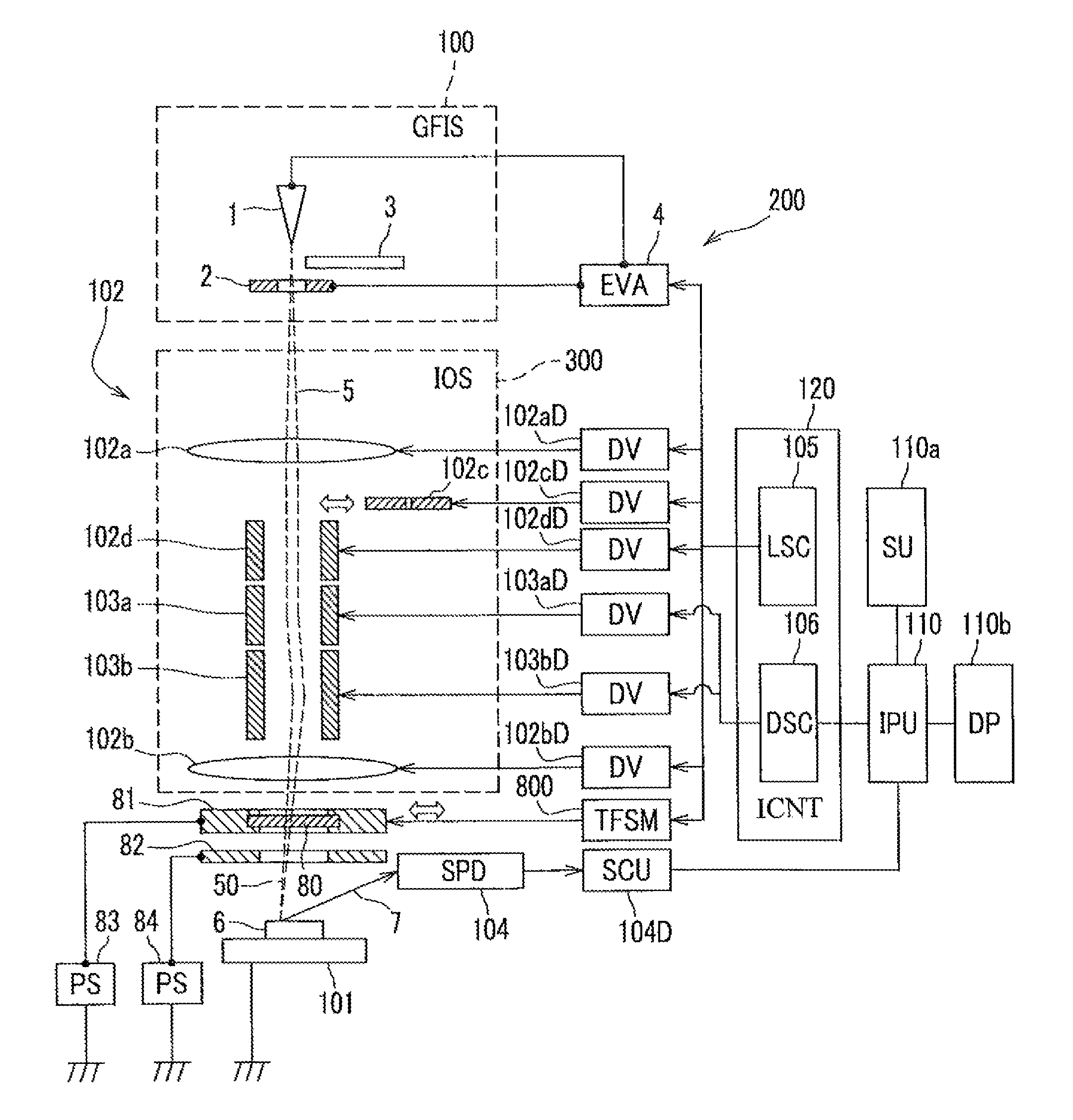
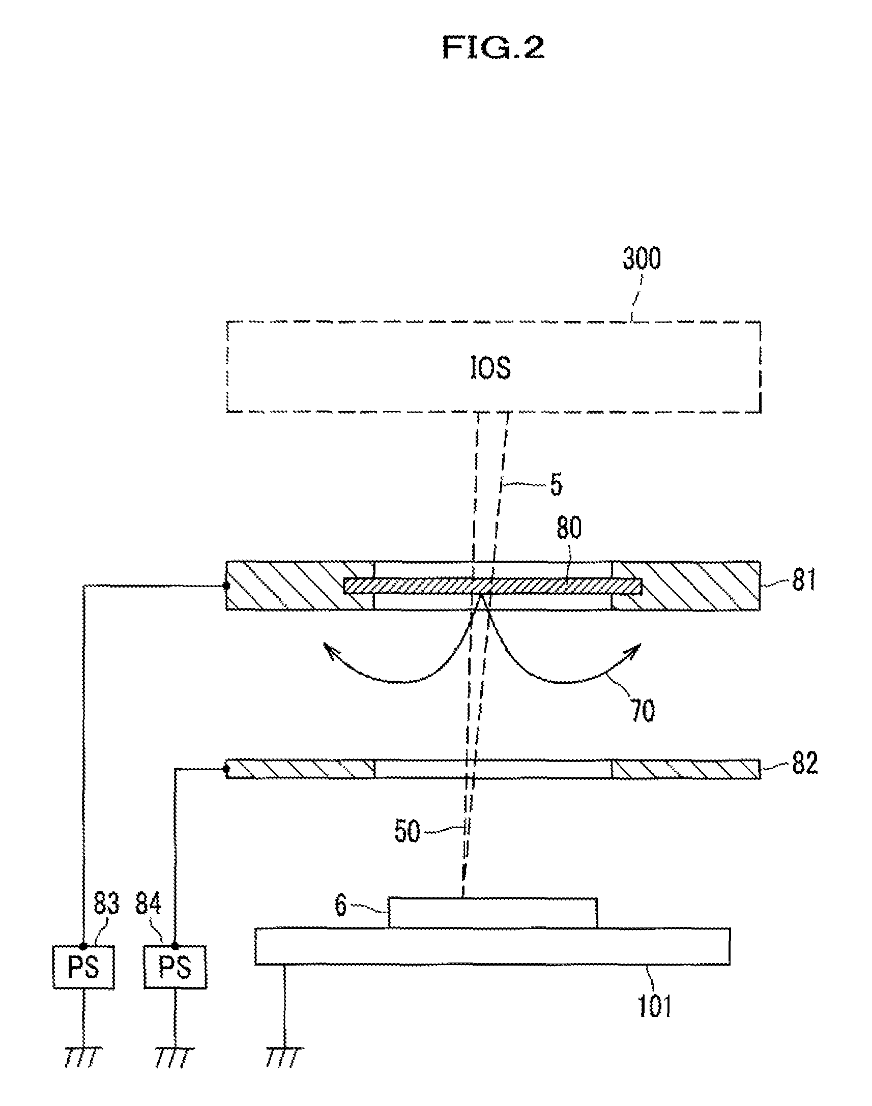
[0072]FIG. 2 shows a configuration near a thin film of the scanning ion microscope according to the present invention. The periphery of the thin film 80 will be described in detail using FIG. 2. When the thin film 80 is irradiated with the ion beam 5, the secondary electrons 70 transmit through the specimen 6 side of the thin film 80 in addition to the uncharged particle beam 50. When the secondary electrons 70 are mixed with the secondary electrons 7 produced at the specimen 6 and are detected by the secondary particle detector 104 (refer to FIG. 1), noise is mixed in the secondary electron observation image of the specimen 6. Accordingly, in the present embodiment, the electric potential of the electrode 82 having an opening in the center is set by the power source 84 appropriately. That is, the secondary electron 70 is sent back to the thin film 80 side by setting the electric potential of the electrode 82 to minus several tens of V with respect to the electric potential of the s...

second embodiment

[0076]FIG. 3 shows a configuration near a thin film of the scanning ion microscope according to the present invention. The scanning ion microscope in the present embodiment is fundamentally the same as that in FIG. 1 but is different in that there are additional elements near the thin film 80. FIG. 3 shows a peripheral portion of the thin film 80.

[0077]If the thin film 80 is irradiated with the ion beam 5, a small amount of reflection particles and secondary electrons 71 are emitted to the side of the ion optical system 300. When they enter an electrostatic lens or a deflector in the ion optical system 300, the operation of the ion optical system 300 may become unstable as a result of inducement of unnecessary electrification onto the insulator portion. Accordingly, in the present embodiment, a shielding body 85 having an opening is arranged above the thin film 80 for blocking the reflection particles and secondary electrons 71. Although a part of the particles enter into the ion op...

fifth embodiment

[0084]FIG. 6 shows a configuration near a thin film of the scanning ion microscope according to the present invention. The scanning ion microscope in the present embodiment is fundamentally the same as that shown in FIG. 1 but is different in the configuration of the thin film 80. FIG. 6 shows a peripheral portion of the thin film 80. In the present embodiment, a crystalline body 80c is used as the thin film 80. Specifically, the thin film 80 is formed by partially reducing the thickness of a single crystal silicon substrate by etching. In addition, there is provided a thin film inclining mechanism 801 so as to enable change in the incident angle of the ion beam 5 onto the thin film 80.

[0085]Here, there is a channeling phenomenon in the transmission of the ion beam through a crystalline body. That is, the channeling phenomenon is a phenomenon that the transmission capability of an ion beam entering in a specific crystal direction is high. The present embodiment adjusts such that the...


PUM


Abstract

The present invention is provided to enable a detailed inspection of a specimen and preventing a distortion of an observation image even when a specimen containing an insulating material is partially charged. For a scanning ion microscope utilizing a gas field ionization ion source, a thin film is disposed between an ion optical system and a specimen, and an ion beam is applied to and transmitted through this thin film in order to focus a neutralized beam on the specimen. Furthermore, an electrode for regulating secondary electrons discharged from this thin film is provided in order to eliminate mixing of noises into an observation image.

Description

FIELD OF THE INVENTION[0001]The present invention relates to a scanning ion microscope that can form a specimen image by scanning with uncharged particles and a secondary particle control method.BACKGROUND ART[0002]Patent Document 1 and Patent Document 2 disclose focused ion beam (FIB) devices that have gas field ionization ion source (GFIS) and use gas ions such as hydrogen (H2), helium (He), and neon (Ne). Such gas focused ion beams (gas FIB) has an advantageous effect in that they do not bring Ga contamination to the specimen as in a gallium (Ga: metal) focused ion beam (Ga-FIB) from a liquid metal ion source (LMIS), which is used often nowadays.[0003]In addition, the energy width of the gas ions extracted from GFIS is narrow and the size of an ion generation source is small in GFIS, and thus GFIS can form minute beams than Ga-FIB.[0004]Such gas FIB devices are used as a scanning ion microscope having a high resolution. That is, an image of the specimen is formed by detecting sec...

Claims


Application Information

Patent Timeline
Patent Type & Authority Patents(United States)
IPC IPC(8): H01J37/26H01J37/22H01J37/244H01J37/20H01J37/28
CPCH01J37/28H01J37/265H01J37/244H01J37/222H01J37/20H01J2237/2806H01J2237/2807H01J2237/0473H01J2237/0807H01J37/317
Inventor KAWANAMI, YOSHIMIOSE, YOICHI
Owner HITACHI HIGH-TECH CORP
Why Eureka
Try Eureka