Film for flip chip type semiconductor back surface, dicing tape-integrated film for semiconductor back surface, process for producing semiconductor device, and flip chip type semiconductor device

a technology of flip chip and back surface, which is applied in the direction of natural mineral layered products, synthetic resin layered products, adhesive types, etc., can solve the problems of increasing the number of processing steps, increasing the production cost, and sometimes damage to semiconductor chips, so as to prevent the generation of warp on the semiconductor element, suppress the effect of semiconductor element damage and prevent the generation of warp

Active Publication Date: 2015-07-07
NITTO DENKO CORP
View PDF26 Cites 2 Cited by
  • Summary
  • Abstract
  • Description
  • Claims
  • Application Information

AI Technical Summary

Benefits of technology

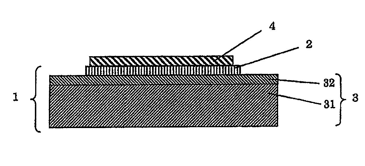
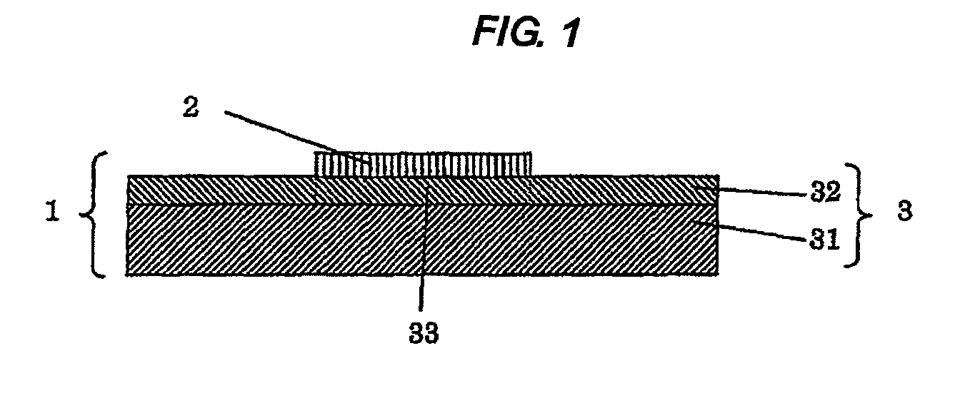
[0019]The film for flip chip type semiconductor back surface of the invention exerts the function of protecting a semiconductor element flip chip-connected onto an adherend when the film is formed on a back surface of the semiconductor element. Moreover, in the film for flip chip type semiconductor back surface of the invention, since 70% by weight or more of an inorganic filler is contained based on the whole of the film for flip chip type semiconductor back surface, tensile storage modulus of the film is relatively high. As a result, the warp of the semiconductor element, which may be generated at the thermal curing of the encapsulating resin, can be effectively suppressed or prevented. Moreover, by controlling the content of the inorganic filler to 95% by weight or less, appropriate flexibility can be imparted to the film. Incidentally, the back surface of the semiconductor element means a surface opposite to the surface thereof on which a circuit is formed.
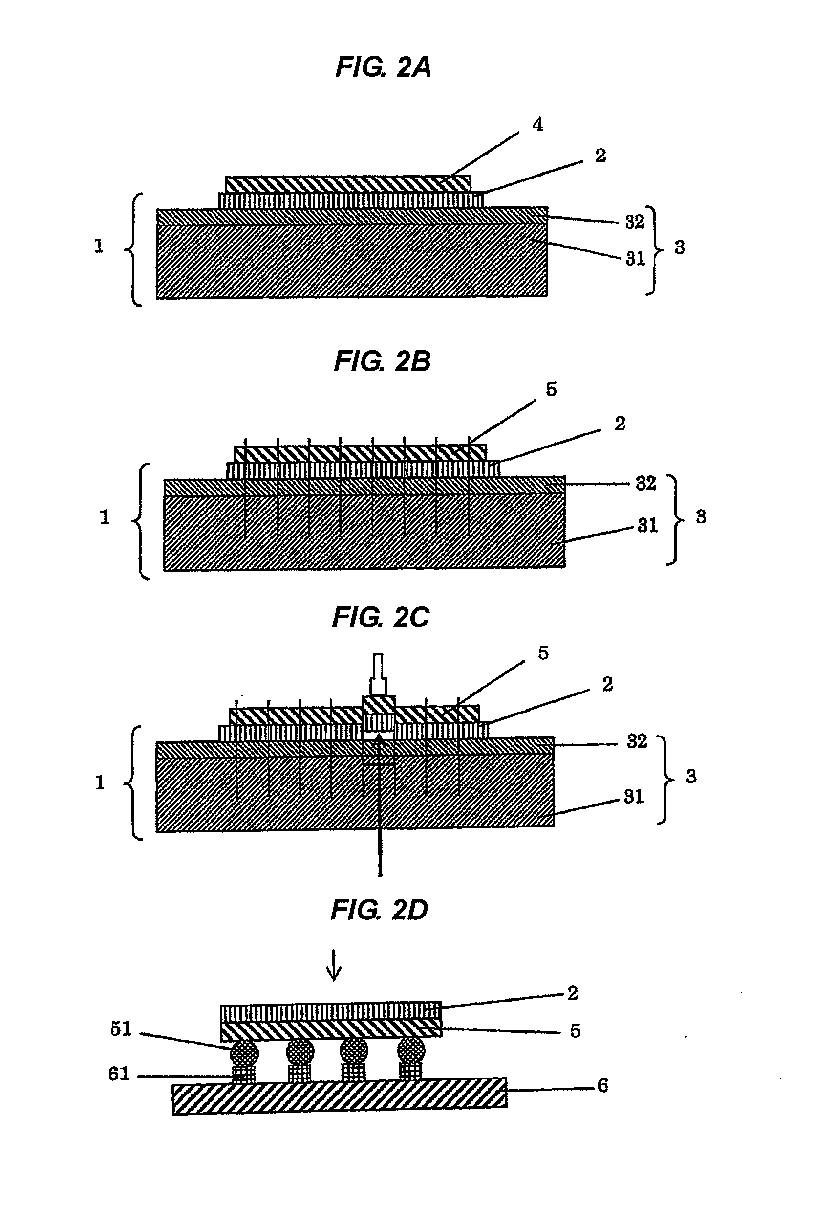
[0031]Furthermore, according to the process for producing the semiconductor device of the invention, since the dicing tape-integrated film for semiconductor back surface is attached to the back surface of the semiconductor wafer and therefore, the step of attaching the film for semiconductor back surface alone is not required. Moreover, since the back surfaces of the semiconductor wafer and the semiconductor element are protected by the film for semiconductor back surface during the dicing of the semiconductor wafer and the picking-up of the semiconductor element formed by the dicing, damaging and the like can be prevented. Also, generation of warp on the semiconductor element can be prevented at the time when the semiconductor element is flip chip-connected onto the adherend. As a result, the flip chip type semiconductor device can be produced with improving the production yield.BRIEF DESCRIPTION OF THE DRAWINGS

Problems solved by technology

However, the protection of the back surface of a semiconductor chip with a protective film requires an additional step of attaching the protective film to the back surface of the semiconductor chip obtained in a dicing step.
As a result, the number of the processing steps increases and the production cost is thereby increased.
Moreover, the recent tendency toward thinning may result in that semiconductor chips are sometimes damaged in the step of picking up the semiconductor chips.

Method used


Image

  • Film for flip chip type semiconductor back surface, dicing tape-integrated film for semiconductor back surface, process for producing semiconductor device, and flip chip type semiconductor device
  • Film for flip chip type semiconductor back surface, dicing tape-integrated film for semiconductor back surface, process for producing semiconductor device, and flip chip type semiconductor device
  • Film for flip chip type semiconductor back surface, dicing tape-integrated film for semiconductor back surface, process for producing semiconductor device, and flip chip type semiconductor device

Examples


example 1

Preparation of Film for Flip Chip Type Semiconductor Back Surface

[0156]40 parts of a phenoxy resin (trade name “EP4250” manufactured by JER Co., Ltd.), 129 parts of a phenol resin (trade name “MEH-8320” manufactured by Meiwa Chemical Co., Ltd.), 663 parts of a spherical silica (trade name “SO-25R” manufactured by Admatechs Company Limited, average particle diameter: 0.5 mm) as an inorganic filler, 14 parts of a dye (trade name “OIL BLACK BS” manufactured by Orient Chemical Industries Co., Ltd.), and 1 part of a thermal curing-accelerating catalyst (trade name “2PHZ-PW” manufactured by Shikoku Chemicals Corporation) based on 100 parts of an epoxy resin (trade name “HP4032D” manufactured by DIC, Inc.) were dissolved in methyl ethyl ketone to prepare a solution of an adhesive composition having a solid concentration of 23.6% by weight.

[0157]The solution of the adhesive composition was applied on a releasably treated film, as a release liner (separator), composed of a polyethylene terep...

example 2

Preparation of Film for Flip Chip Type Semiconductor Back Surface

[0159]40 parts of a phenoxy resin (trade name “EP4250” manufactured by JER Co., Ltd.), 129 parts of a phenol resin (trade name “MEH-8320” manufactured by Meiwa Chemical Co., Ltd.), 1137 parts of a spherical silica (trade name “SO-25R” manufactured by Admatechs Company Limited, average particle diameter: 0.5 μm), 14 parts of a dye (trade name “OIL BLACK BS” manufactured by Orient Chemical Industries Co., Ltd.), and 1 part of a thermal curing-accelerating catalyst (trade name “2PHZ-PW” manufactured by Shikoku Chemicals Corporation) based on 100 parts of an epoxy resin (trade name “HP4032D” manufactured by DIC, Inc.) were dissolved in methyl ethyl ketone to prepare a solution of an adhesive composition having a solid concentration of 23.6% by weight.

[0160]The solution of the adhesive composition was applied on a releasably treated film, as a release liner (separator), composed of a polyethylene terephthalate film having a...


PUM

PropertyMeasurementUnit
thicknessaaaaaaaaaa
thicknessaaaaaaaaaa
thicknessaaaaaaaaaa

Abstract

The present invention relates to a film for flip chip type semiconductor back surface to be formed on a back surface of a semiconductor element flip chip-connected to an adherend, the film for flip chip type semiconductor back surface containing an inorganic filler in an amount within a range of 70% by weight to 95% by weight based on the whole of the film for flip chip type semiconductor back surface.

Description

FIELD OF THE INVENTION[0001]The present invention relates to a film for flip chip type semiconductor back surface and a dicing tape-integrated film for semiconductor back surface. The film for flip chip type semiconductor back surface is used for the purposes of protecting a back surface of a semiconductor element such as a semiconductor chip and enhancing strength thereof and the like. Also, the invention relates to a process for producing a semiconductor device using a dicing tape-integrated film for semiconductor back surface and a flip chip type semiconductor device.BACKGROUND OF THE INVENTION[0002]Recently, thinning and miniaturization of a semiconductor device and its package have been increasingly demanded. Therefore, as the semiconductor device and its package, flip chip type semiconductor devices in which a semiconductor element such as a semiconductor chip is mounted (flip chip-connected) on a substrate by means of flip chip bonding have been widely utilized. In such flip ...

Claims


Application Information

Patent Timeline
Patent Type & Authority Patents(United States)
IPC IPC(8): H01L23/48C09J163/00
CPCC09J163/00H01L2224/16225H01L2924/0002H01L2924/00H01L21/30H01L21/78
Inventor TAKAMOTO, NAOHIDESHIGA, GOJIASAI, FUMITERU
Owner NITTO DENKO CORP
Why Eureka
Try Eureka