Luminescent element including nitride, preparation method thereof and luminescence method
a technology of luminescent elements and nitride, which is applied in the field of luminescent materials, can solve the problems of limiting the application of field emission devices, especially illumination, and low luminous efficiency, and achieves the effects of high internal quantum efficiency low efficiency problem of the luminescent material, and high spontaneous emission of the luminescent substra
- Summary
- Abstract
- Description
- Claims
- Application Information
AI Technical Summary
Benefits of technology
Problems solved by technology
Method used
Image
Examples
example 1
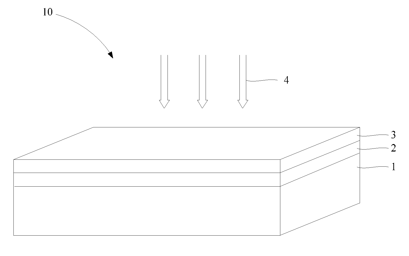
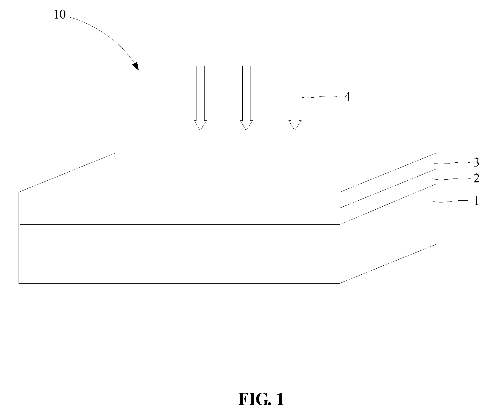
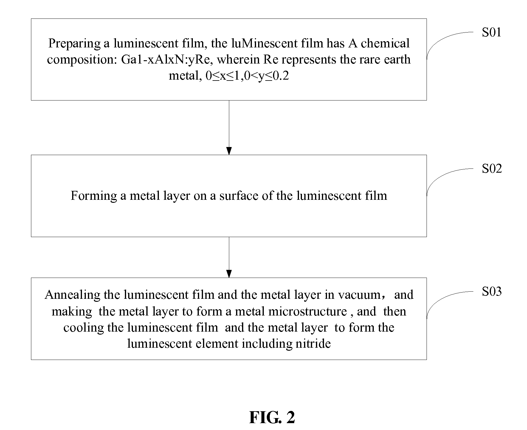
[0036]A 1×1 cm2, double-side polished substrate made of quartz is selected, then a luminescent film is formed on a surface of the substrate by magnetron sputtering, and the luminescent film has the composition of AlN:0.005Tm. The luminescent film is test by XRD, and the test result is shown in FIG. 4. In FIG. 4, the film exhibits (002) preferential growth, and crystallographic orientation of aluminum nitride is obtained. A silver layer with a thickness of 2 nm is deposited on a surface of the luminescent film via a magnetron sputtering equipment. The substrate, the luminescent film, and the silver layer are annealed at a temperature of 300° C. for half an hour in vacuum with the vacuum degree −3 Pa and cooled to ambient temperature, thus a luminescent element including nitride is obtained. Structure of the luminescent element including nitride doped the rare earth element shown in FIG. 1, wherein the substrate 1 is made of quartz, the luminescent film 2 has the composition of AlN:0....
example 2
[0039]A 1×1 cm2, double-side polished substrate made of quartz is selected, then a luminescent film is formed on a surface of the substrate by electron beam evaporating, and the luminescent film has the composition of Ga0.5Al0.5N:0.2Tb. A golden layer with a thickness of 0.5 nm is deposited on a surface of the luminescent film via a magnetron sputtering equipment. The substrate, the luminescent film, and the golden layer are annealed at a temperature of 200° C. for an hour in vacuum with the vacuum degree −3 Pa and cooled to ambient temperature, thus a luminescent element including nitride is obtained.
example 3
[0040]A 1×1 cm2, double-side polished substrate made of sapphire is selected, then a luminescent film is formed on a surface of the substrate by chemical vapor deposition, and the luminescent film has the composition of Ga0.2Al0.8N:0.06Gd. A aluminum layer with a thickness of 200 nm is deposited on a surface of the luminescent film via a magnetron sputtering equipment. The substrate, the luminescent film, and the aluminum layer are annealed at a temperature of 500° C. for 5 hours in vacuum with the vacuum degree −3 Pa and cooled to ambient temperature, thus a luminescent element including nitride is obtained.
PUM
| Property | Measurement | Unit |
|---|---|---|
| temperature | aaaaa | aaaaa |
| operating temperature | aaaaa | aaaaa |
| weight percent | aaaaa | aaaaa |
Abstract
Description
Claims
Application Information
 - R&D
- Intellectual Property
- Life Sciences
- Materials
- Tech Scout
- Unparalleled Data Quality
- Higher Quality Content
- 60% Fewer Hallucinations
Browse by: Latest US Patents, China's latest patents, Technical Efficacy Thesaurus, Application Domain, Technology Topic, Popular Technical Reports.
© 2025 PatSnap. All rights reserved.Legal|Privacy policy|Modern Slavery Act Transparency Statement|Sitemap|About US| Contact US: help@patsnap.com


