
Power supply device for high frequency power amplification circuit and high frequency power amplification device

a power supply device and high frequency power amplification technology, applied in the direction of electric variable regulation, process and machine control, instruments, etc., can solve the problems of high speed switching, distortion in waveform, complex circuit and extremely complex control, etc., to achieve high speed control, secure a large dynamic range, and high precision

Active Publication Date: 2015-09-29
MURATA MFG CO LTD
View PDF15 Cites 8 Cited by
  • Summary
  • Abstract
  • Description
  • Claims
  • Application Information

AI Technical Summary

Benefits of technology

The present invention provides a power supply device and a high frequency power amplification device that can follow the envelope of a high frequency signal with a simple configuration. The device includes a bidirectional converter that can supply and regenerate electric charges and carry out non-linear control of the ON / OFF times of an internal switching device. This enables high speed control and high accuracy adjustment of the amplitude and phase of the output voltage with high precision, regardless of the range. The technical effect of the invention is a more efficient and effective high frequency power amplification device.

Problems solved by technology

An example of an audio amplification circuit is a class-D amplification circuit (digital amplifier), but in a power supply device for a high frequency power amplification circuit, a frequency band to be handled is a high frequency band, and thus extremely high speed switching is required.
Thus, a complex circuit and extremely complex control are required to repair a voltage difference (waveform step) occurring when switching among the plurality of voltage sources.
If this repair of the waveform step is incomplete, distortion in the waveform increases, and an adjacent channel leakage power ratio (ACPR) in a communication system increases.
Thus, frequencies outside a stipulated range are negatively affected, leading to a problem that the high frequency power amplification device cannot be applied to a product having strict frequency band allocation.

Method used


Image

  • Power supply device for high frequency power amplification circuit and high frequency power amplification device
  • Power supply device for high frequency power amplification circuit and high frequency power amplification device
  • Power supply device for high frequency power amplification circuit and high frequency power amplification device

Examples


first preferred embodiment

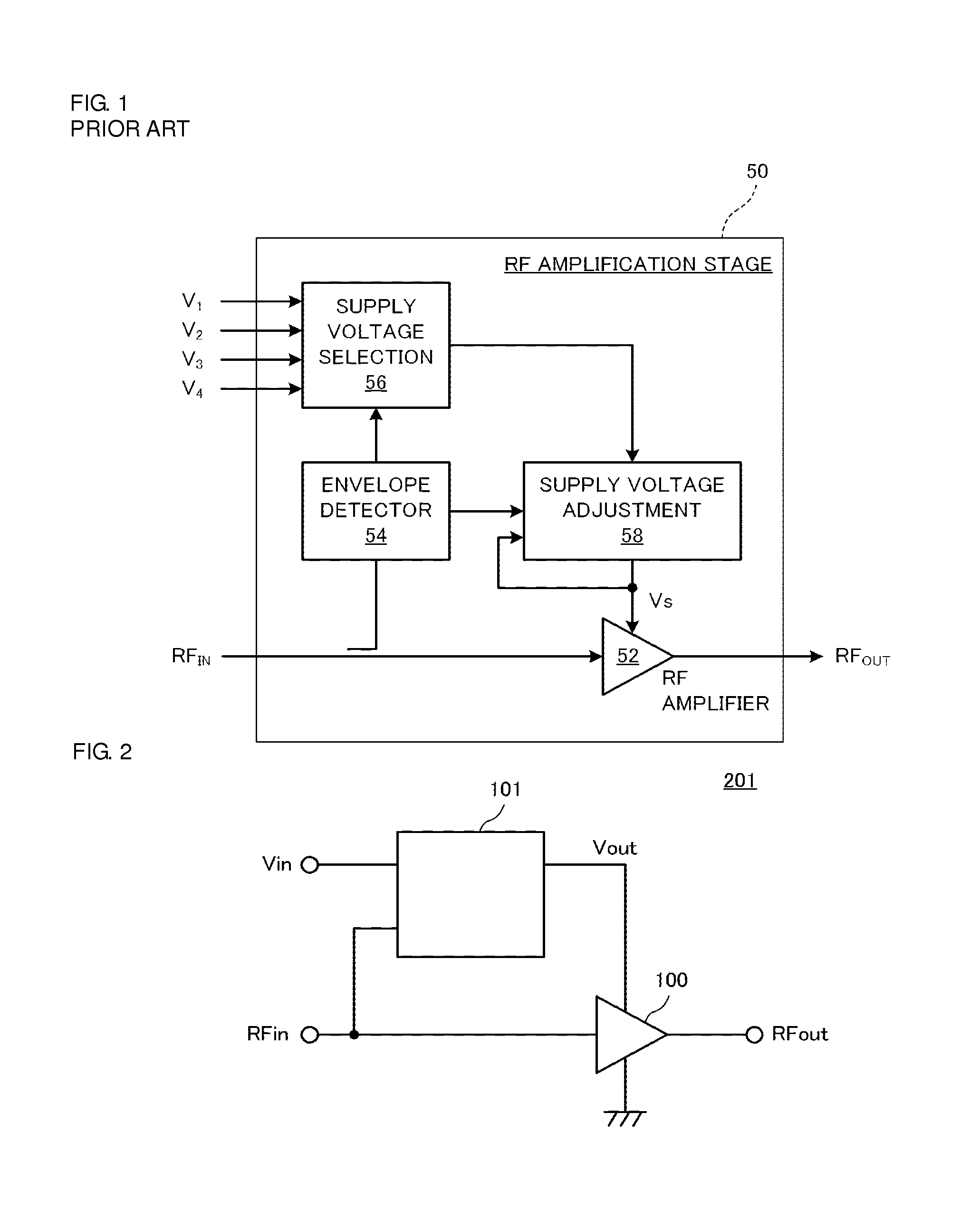
[0050]FIG. 2 is a diagram illustrating the relationship among a power supply device 101 for a high frequency power amplification circuit, a high frequency power amplification device 201, and a high frequency power amplification circuit 100 according to a first preferred embodiment of the present invention.

[0051]The high frequency power amplification circuit 100 receives a high frequency signal RFin as an input, amplifies the power thereof, and outputs a high frequency power signal RFout. The power supply device 101 for a high frequency power amplification circuit receives an input power supply voltage Vin as an input and detects an amplitude change (envelope) of the high frequency signal RFin. The power supply device 101 then varies an output voltage Vout so as to follow the amplitude change. The high frequency power amplification circuit 100 operates with the output voltage Vout of the power supply device 101 for a high frequency power amplification circuit serving as a power suppl...

second preferred embodiment

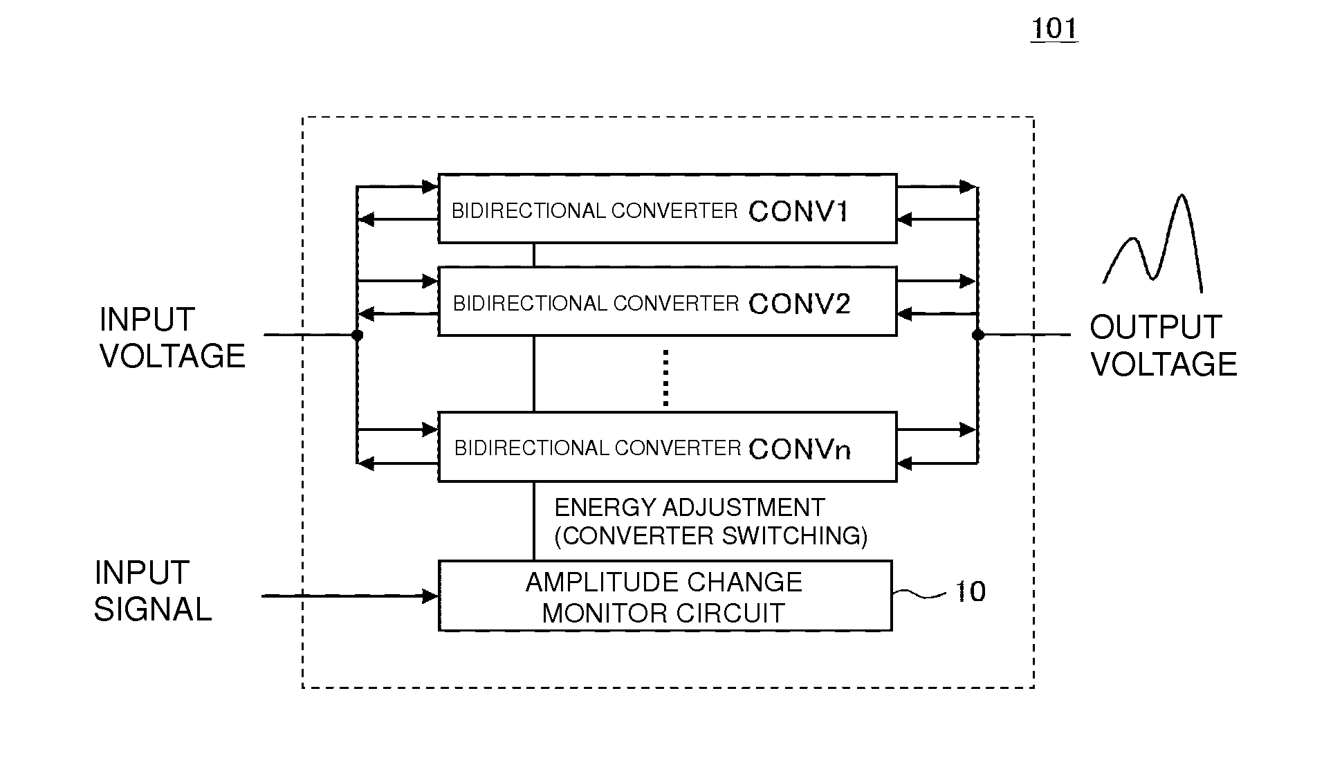
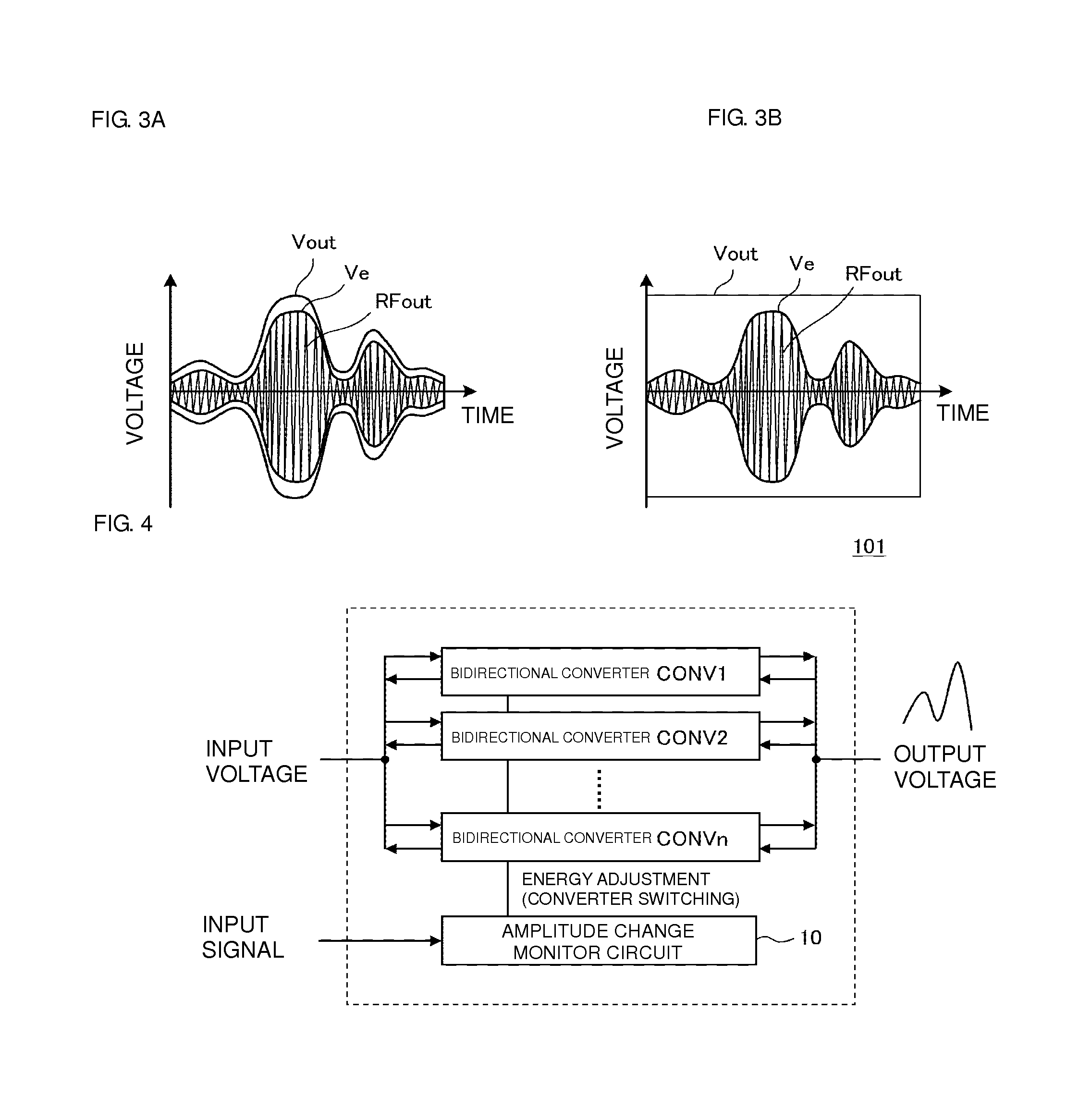
[0058]FIG. 7 is a block diagram illustrating the configuration of a power supply device 102 for a high frequency power amplification circuit according to a second preferred embodiment of the present invention. The plurality of bidirectional converters CONV1, CONV2, . . . , CONVn are provided between the input section for the input voltage and the output section for the output voltage. Each of these bidirectional converters is a converter that is capable of supplying and regenerating an electric charge. Right and left arrows at the input and output sections indicate the energy transfer directions. The amplitude change monitor circuit 10 receives, as an input, an input signal, which is an amplitude change signal (envelope) of a high frequency signal. The amplitude change monitor circuit 10 then controls the supply and regeneration of electric charges in the bidirectional converters CONV1, CONV2, . . . , CONVn so that the output voltage follows the input signal. An output side energy s...

third preferred embodiment

[0061]FIG. 8 is a block diagram illustrating the configuration of a power supply device 103 for a high frequency power amplification circuit according to a third preferred embodiment of the present invention. The plurality of bidirectional converters CONV1, CONV2, . . . , CONVn are provided between the input section for the input voltage and the output section for the output voltage. Each of these bidirectional converters is a converter that is capable of supplying and regenerating an electric charge. Right and left arrows at the input and output sections indicate the energy transfer directions. The amplitude change monitor circuit 10 receives, as an input, an input signal, which is an amplitude change signal of a high frequency signal. The amplitude change monitor circuit 10 then controls the supply and regeneration of electric charges in the bidirectional converters CONV1, CONV2, . . . , CONVn so that the output voltage follows the amplitude change of the high frequency signal. In...


PUM


Abstract

In a power supply device, bidirectional converters that are each capable of supplying or regenerating an electric charge are provided between an input section for an input voltage and an output section for an output voltage. An amplitude change monitor circuit detects an envelope of an RF input signal. A converter switching circuit controls supply and regeneration of electric charges by the bidirectional converters so that the output voltage follows an amplitude change of the input signal. An output capacitor capacitance estimation unit estimates the capacitance of an output capacitor from its voltage and current. A delay time detection circuit grasps a delay time of a power supply device for a high frequency power amplification circuit and makes an adjustment through a delay adjustment circuit.

Description

BACKGROUND OF THE INVENTION[0001]1. Field of the Invention[0002]The present invention relates to power supply devices for high frequency power amplification circuits. In particular, the present invention relates to a power supply device that improves power efficiency of a high frequency power amplification circuit and to a high frequency power amplification device that includes such a power supply device.[0003]2. Description of the Related Art[0004]Japanese Unexamined Patent Application Publication No. 2006-514472 describes a configuration in which, in order to enhance the efficiency of a high frequency amplification circuit, a power supply voltage of the high frequency amplification circuit is caused to follow an amplitude change (envelope) of a high frequency signal to be amplified. The frequency of the amplitude change of the high frequency signal here is not a carrier wave frequency (e.g., 1 GHz to 2 GHz in cellular phones) but is the frequency (approximately 10 MHz to 100 MHz) ...

Claims


Application Information

Patent Timeline
Patent Type & Authority Patents(United States)
IPC IPC(8): H03G3/20H03F3/189H03F1/02H03F3/21H03F3/24H04B1/04H02M3/158
CPCH03F1/0222H02M3/1584H03F1/025H03F3/189H03F3/21H03F3/245H04B1/0475H02M3/1582H03F2200/102H03F2200/451H03F2200/504H03F2200/507H03F2200/511H03F2200/516H04B2001/045H03F1/02H03F3/24
Inventor TSUJI, HITOSHI
Owner MURATA MFG CO LTD
Learn More