

Resist composition and patterning process
a composition and patterning technology, applied in the field of resist composition, can solve the problems of acid diffusion, poor etch resistance and substantial outgassing, image blur, etc., and achieve the effect of minimal edge roughness and high resolution
Active Publication Date: 2015-10-20
SHIN ETSU CHEM CO LTD
View PDF34 Cites 8 Cited by
- Summary
- Abstract
- Description
- Claims
- Application Information
AI Technical Summary
Benefits of technology
The composition achieves high resolution and sensitivity with minimal LER, is suitable for VLSI and photomask fabrication, and eliminates the need for antistatic films, using non-toxic solvents for improved coating uniformity and reduced outgassing.
Problems solved by technology
As the feature size is reduced, image blurs due to acid diffusion become a problem (see Non-Patent Document 1).
Due to the lack of cyclic structure, it has the drawbacks of poor etch resistance and substantial outgassing during exposure.
The EB writing of a resist film encounters a problem that the point of writing is shifted by electrostatic charges on the resist film.
Undesirably coating of the antistatic film adds to the cost of the overall process.
It was impossible to use metal-containing materials as the photoresist material for the semiconductor lithography because of a possible malfunction of semiconductor devices as a result of metal atoms migrating to the substrate.
These solvents, however, cannot be used in the industrial application because of their toxicity.
In addition, these solvents having low boiling points have so high evaporation rates during spin coating that they may dry up during film formation before the coating thickness becomes uniform.
The lack of coating thickness uniformity is a problem.
In the cited documents, development uses resist solvents, which also suffer from the toxic problem.
Method used
View moreImage
Smart ImageViewing Examples

Examples
example
[0062]Examples of the invention are given below by way of illustration and not by way of limitation. The abbreviation “pbw” is parts by weight. The weight average molecular weight (Mw) and the number average molecular weight (Mn) are the value by GPC versus polystyrene standard.
Login to View More PUM
| Property | Measurement | Unit |
|---|---|---|
| wavelength | aaaaa | aaaaa |
| thickness | aaaaa | aaaaa |
| thickness | aaaaa | aaaaa |
Abstract
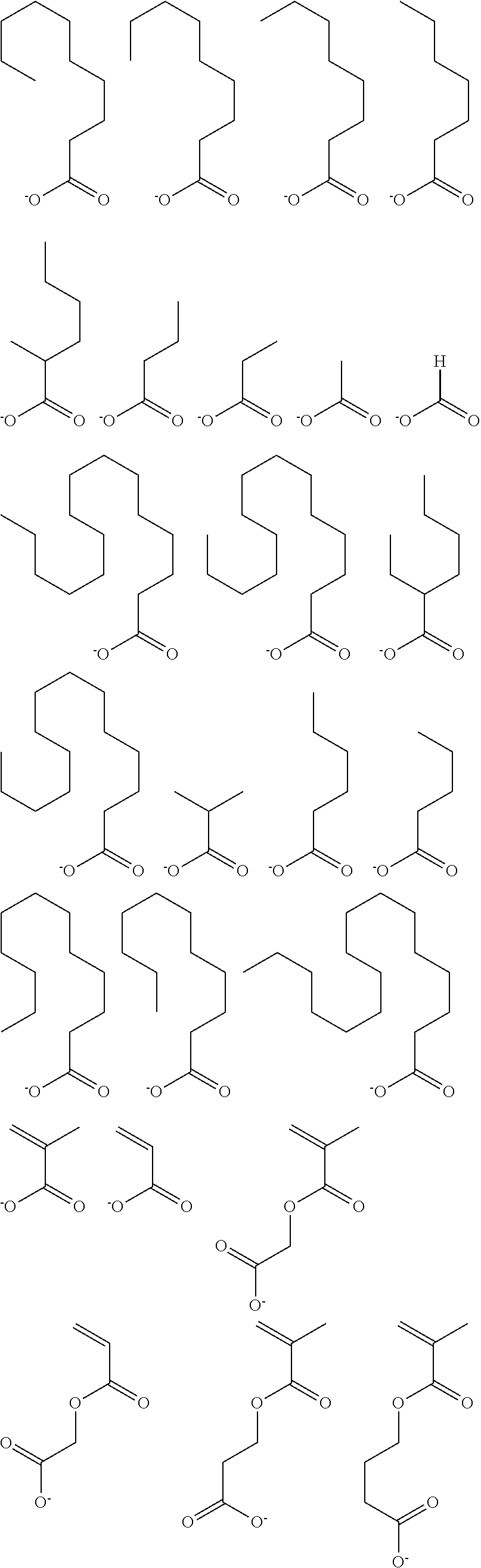
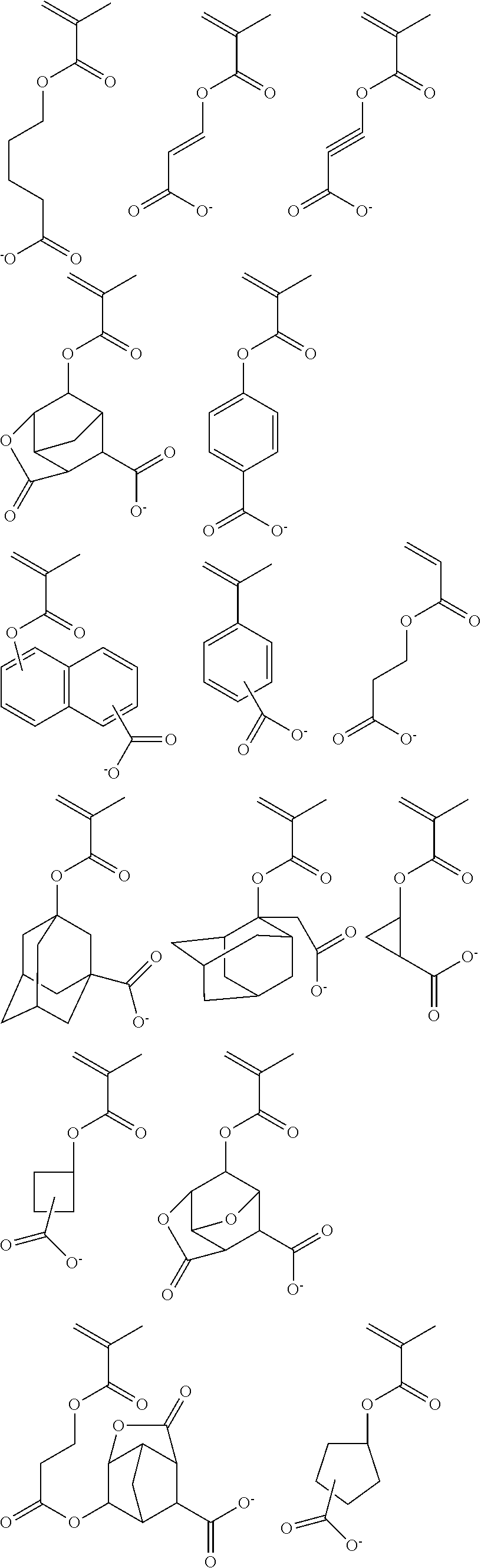
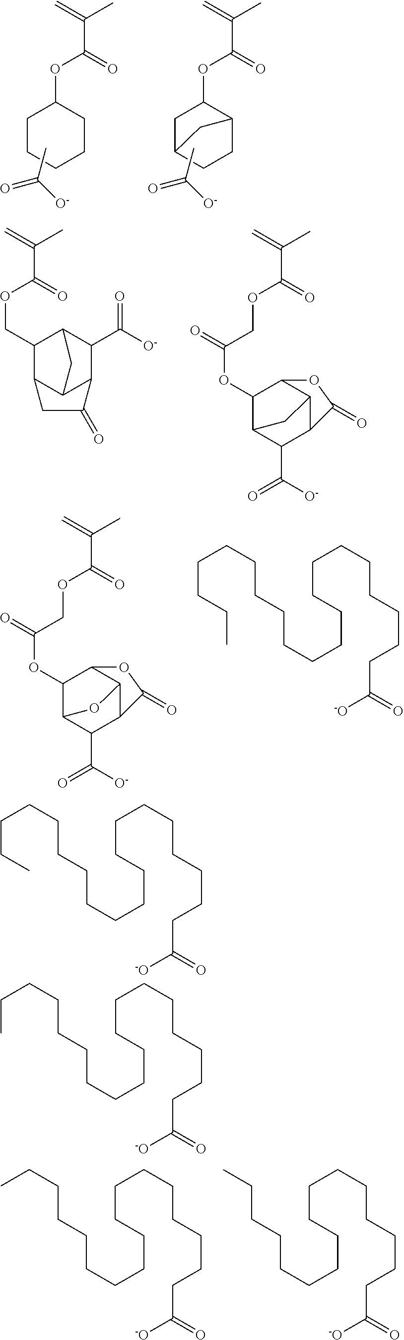
A resist composition comprising a salt of a mono- to tetrafunctional carboxylic acid with a metal selected from magnesium, chromium, manganese, iron, cobalt, nickel, copper, zinc, silver, cadmium, indium, tin, antimony, cesium, zirconium, and hafnium, and a solvent is improved in film uniformity when coated, and exhibits a high resolution, high sensitivity, and minimal LER when processed by the EB or EUV lithography.
Description
CROSS-REFERENCE TO RELATED APPLICATION[0001]This non-provisional application claims priority under 35 U.S.C. §119(a) on Patent Application No. 2011-029588 filed in Japan on Feb. 15, 2011, the entire contents of which are hereby incorporated by reference.TECHNICAL FIELD[0002]This invention relates to a resist composition, and more particularly to a negative resist composition adapted for the EB and EUV lithography processes; and a patterning process using the same.BACKGROUND ART[0003]To meet the demand for higher integration density and operating speed of LSIs, the effort to reduce the pattern rule is in rapid progress. The wide-spreading flash memory market and the demand for increased storage capacities drive forward the miniaturization technology. As the advanced miniaturization technology, manufacturing of microelectronic devices at the 65-nm node by the ArF lithography has been implemented in a mass scale. Manufacturing of 45-nm node devices by the next generation ArF immersion ...
Claims
Login to View More Application Information
Patent Timeline
 Patent Type & AuthorityPatents(United States)
IPC IPC(8): G03F7/004G03F7/038G03F7/075
CPCG03F7/038G03F7/0043G03F7/0048G03F7/0757
InventorHATAKEYAMA, JUN
OwnerSHIN ETSU CHEM CO LTD