Self-adaptive composite tunneling field effect transistor and method for fabricating the same

a composite tunneling and field effect transistor technology, applied in the direction of semiconductor devices, basic electric elements, electrical appliances, etc., can solve the problems of increasing the power consumption of the device, increasing the leakage current, increasing the off-state leakage current of the device, etc., to facilitate band-to-band tunneling, improve the on-state current, and improve the effect of performan

Inactive Publication Date: 2015-10-27
PEKING UNIV
View PDF10 Cites 3 Cited by
  • Summary
  • Abstract
  • Description
  • Claims
  • Application Information

AI Technical Summary

Benefits of technology

[0005]An object of the present invention is to provide a tunneling field effect transistor with a composite mechanism by combining a current of a MOSFET in a self-adaptive way and a method for fabricating the same. The transistor of the invention can be completely compatible with the conventional CMOS process, a turning-on current of the TFET can be dramatically increased and a steeper subthreshold characteristics can be obtained while an ambipolar effect can be suppressed.
[0020]I. An asymmetric TFET structure having good performance can be formed through the secondarily highly doped region in the source region, the relatively lightly doped drain region and the control gate. On one hand, since the secondary doping for the source region is a high doping implantation, the preliminarily doped impurities can be effectively compensated and thus impurities having an opposite doping type can be formed so as to form the TFET structure. Furthermore, since the types of the preliminarily and secondarily doped impurities are opposite to each other, a concentration gradient at a tunneling junction of the TFET can become steeper due to a depletion effect and thus facilitate a band-to-band tunneling, so that a steeper subthreshold slope and a higher on-state current compared with the conventional TFET can be obtained. On the other hand, since the doping in the drain region is achieved during the preliminary self-alignment implantation, the doping concentration of the drain region is relatively low, so that an ambipolar effect occurred in the conventional TFET can be effectively inhibited and an ambipolar turning-on current can be suppressed. Therefore, the design of the preliminarily and secondarily implantations by using different concentrations and doping at different locations can obtain a steeper subthreshold characteristic while suppressing the ambipolar effect of the TFET.
[0021]II. A design that the secondarily doped region is spaced apart from the edges of the active region in a width direction at a certain interval can effectively introduce the trait of MOSFET to the transistor according to the invention. On one hand, in the transistor of the invention, a MOSFET is formed through a portion of the source region that is not implanted by the secondary doping, the control gate and the drain source. Thus, such structure can obtain much higher turning-on current than that of the conventional TFET in the same area of the active region. On the other hand, since the interval is smaller than the depletion width, an energy band at a source junction of the MOSFET portion is raised up, so that the MOSFET portion is not easily to be turned on. Thus, under a condition that steps of processes are not increased, the TFET portion can be turned on earlier than the MOSFET portion through simple layout designs by automatically adjusting threshold voltages of the TFET and the MOSFET. As such, the subthreshold characteristic of the transistor can be determined by the TFET so that it is not limited by the subthreshold slope limitation of the conventional MOSFET. Therefore, the transistor combines the advantages of the conventional TFET and MOSFET very well, a better subthreshold characteristic and a higher on-state current can be obtained, so that the transistor can self-adaptively achieve a composite mechanism combination.
[0022]III. The transistor according to the invention has simple fabrication processes, which are completely compatible with the conventional MOSFET processes. The performance of the transistor can be greatly enhanced without increasing the area of the active region and the process complexity.
[0023]In short, the transistor according to the invention employs a design that the source region is doped with two different concentrations and a certain interval is left with respect to locations, a trait of the large turning-on current in the MOSFET can be effectively combined to increase the on-state current of the transistor according to the invention, and a threshold adjustment for the MOSFET portion and the TEFT portion can be achieved in a self-adaptive way. When compared with the conventional TFET, a higher turning-on current and a lower subthreshold slope can be obtained by the transistor of the invention under the same process condition and the same size of the active region, so that it can be used in low power applications. Thus, the transistor according to the invention has a high practical value.

Problems solved by technology

With the size of a MOSFET shrinks, the device is subjected to even more severe negative effects such as a short channel effect of the device and etc. after entering a nanometer scale, which causes an off-state leakage current of device increase.
Meanwhile, since a subthreshold slope of a conventional MOSFET is limited by the thermoelectric potential and thus cannot be reduced synchronously as the size of device decreases, there is a theoretical limit at 60 mV / dec, causing that the leakage current further increases as the reduction of the supply voltage, and thereby increasing the power consumption of the device.
The power consumption issue has now become one of the most serious problems in limiting the scaling down of the device.
However, the TFET faces a problem of a small on-state current due to constraints in the tunneling probability and tunneling area of a source junction, which is far less desirable than that of traditional MOSFET.
Moreover, the TFET has an ambipolar effect, greatly limiting the application of the TFET.

Method used


Image

  • Self-adaptive composite tunneling field effect transistor and method for fabricating the same
  • Self-adaptive composite tunneling field effect transistor and method for fabricating the same
  • Self-adaptive composite tunneling field effect transistor and method for fabricating the same

Examples


Embodiment Construction

[0041]Hereinafter, the present invention will be further described through examples. It is noted that the embodiment is disclosed for the purposes of further understanding of the present invention. However, it is appreciated to those skilled in the art that various substitutions and modifications are possible without departing from the spirit and scope of the invention and the accompanying claims. Therefore, the present invention is not limited to the disclosure of the embodiments, but based on the scope defined by the claims.

[0042]An embodiment of the fabrication method according to the present invention includes processes shown in FIG. 1 to FIG. 4b.

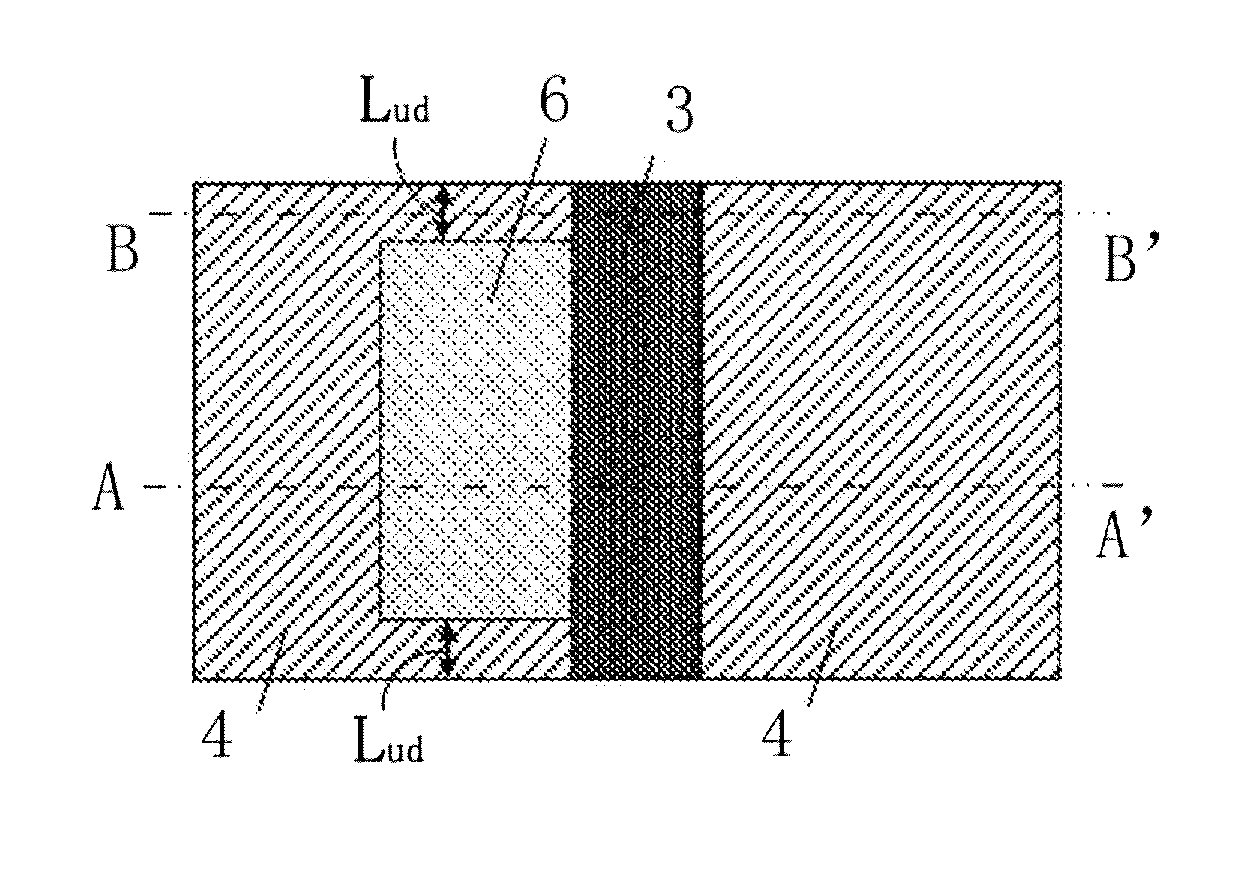
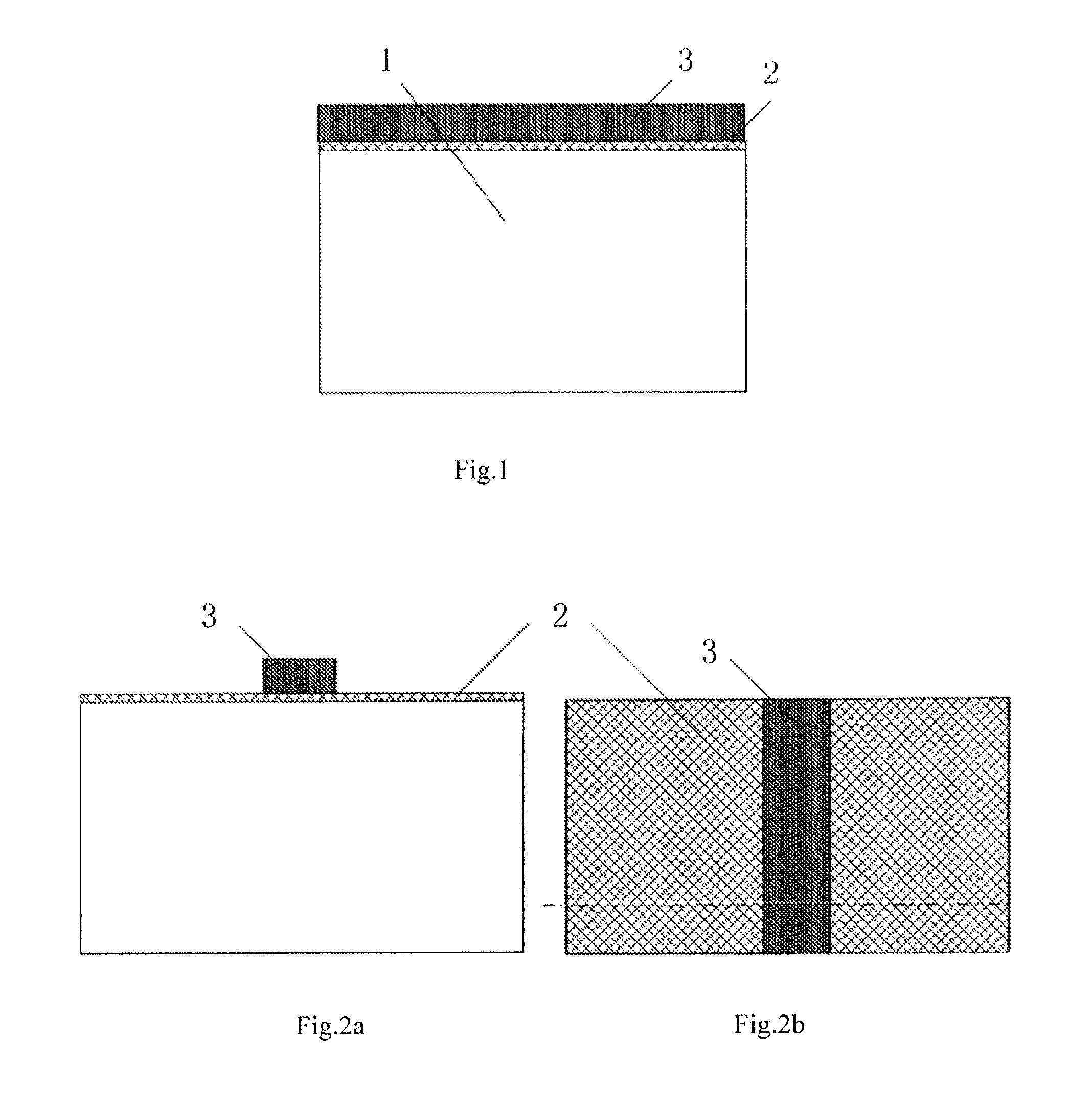
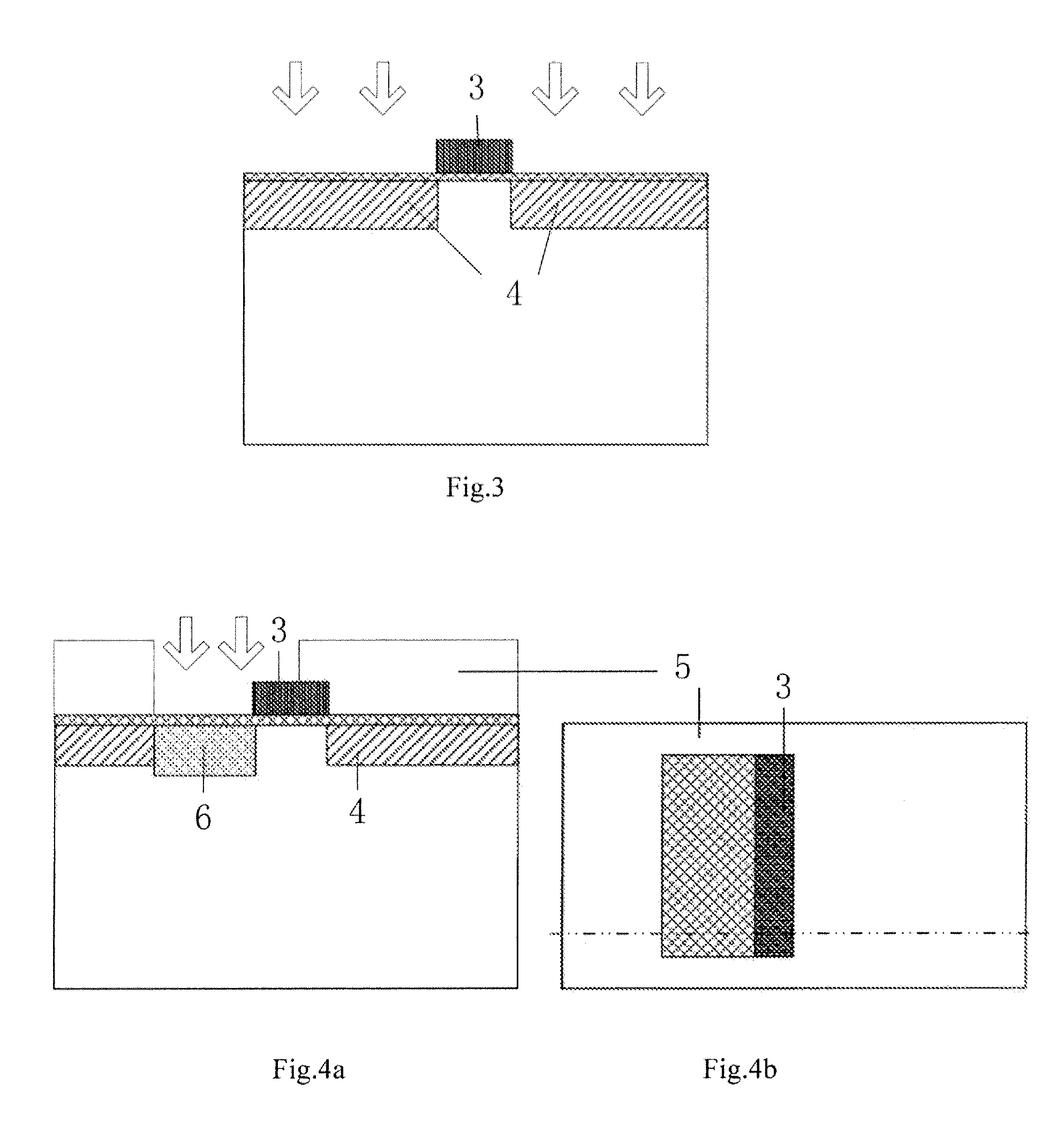
[0043]1. As shown in FIG. 1, an isolation layer for an active region is fabricated by using a shallow isolation technology on a bulk silicon wafer substrate 1, which has a crystal orientation of (100). The substrate is lightly doped. Subsequently, a gate dielectric layer 2 is grown by a thermal growth process. The gate dielectric layer...


PUM


Abstract

The present invention provides a tunneling field effect transistor and a method for fabricating the same which refer to a field effect transistor logic device and circuit in a CMOS ultra-large integrated circuit (ULSI). The inventive concept of the invention lies in that, in a case of an N-type transistor, a side portion of a doped source region adjacent to an edge of the control gate is further implanted with P+ impurities on a basis of the doped source region being initially doped N− impurities, so that the initial N− impurities in the implanted portion are completely compensated by the P+ impurities, and in a case of a P-type transistor, a side portion of the doped source region adjacent to an edge of the control gate is implanted with N+ impurities on a basis of the doped source region being initially doped P− impurities, so that the initial P− impurities in the implanted portion are completely compensated by the N+ impurities. In the transistor, the source region is implanted twice with different doping concentrations, such that a large current characteristic of the MOSFET can be effectively combined to increase an on-state current of the transistor, and also, the threshold adjustment for the MOSFET portion and the TFET portion of the transistor can be achieved in a self-adaptive way.

Description

CROSS REFERENCE TO RELATED APPLICATIONS[0001]The present application is a national stage application under 35 U.S.C. §371 of International Application No. PCT / CN2013 / 074876, filed Apr. 27, 2013, which in turn claims priority to Chinese application No. 201210139560.6, filed May 8, 2012, the contents of each of which are incorporated herein by reference in their entireties.FIELD OF THE INVENTION[0002]Then present invention refers to a field effect transistor logic device and circuit in a CMOS ultra large integrated circuit (ULSI), and in particular, refers to a tunneling field effect transistor (TFET) by effectively combining with a current of a metal-oxide-silicon field effect transistor (MOSFET) in a self-adaptive way and a method for fabricating the same.BACKGROUND OF THE INVENTION[0003]With the size of a MOSFET shrinks, the device is subjected to even more severe negative effects such as a short channel effect of the device and etc. after entering a nanometer scale, which causes a...

Claims


Application Information

Patent Timeline
Patent Type & Authority Patents(United States)
IPC IPC(8): H01L29/06H01L21/28H01L21/324H01L21/266H01L21/265H01L29/739H01L29/08H01L29/66
CPCH01L29/66977H01L21/266H01L21/26513H01L21/28194H01L21/28202H01L21/28211H01L21/324H01L29/0649H01L29/0847H01L29/66325H01L29/7391H01L21/823807H01L21/823814
Inventor HUANG, RUHUANG, QIANQIANZHAN, ZHANQIU, YINGXINWANG, YANGYUAN
Owner PEKING UNIV
Why Eureka
Try Eureka