Sub-threshold FPGA and related circuits and methods thereof

a technology of sub-threshold and related circuits, applied in the field of sub-threshold fpga, can solve the problems of high design complexity, low energy efficiency, and high cost of developing these applications, and achieve the effects of reducing fpga area, low energy overhead, and optimizing routing delay

Active Publication Date: 2015-11-03
UNIV OF VIRGINIA ALUMNI PATENTS FOUND
View PDF16 Cites 4 Cited by
  • Summary
  • Abstract
  • Description
  • Claims
  • Application Information

AI Technical Summary

Benefits of technology

[0005]An aspect of an embodiment of the present invention provides a sub-VT FPGA that uses a low swing, dual-VDD interconnect scheme to reduce FPGA area per LUT, delay at a constant energy, and energy at a constant delay relative to a conventional design at low voltage. These improvements are made possible by, among other things, a custom asynchronous sense amp, a separated voltage for memory cells, and an improved passgate interconnect to optimize routing delay with low energy overhead. This sub-threshold FPGA design enables energy efficient and cost effective configurable logic for a wide variety of ULP applications.
[0007]Since the global interconnect is costly in energy and delay, an aspect of an embodiment of the present FPGA invention, among other things, increases the utilization of local routing available inside clustered configurable logic blocks (CLBs) to reduce global signal traffic. Since more clustering increases local connections for any given configuration, it reduces the number of hops required on the global fabric, which is helpful to Applicant's low swing circuit approach. Multiple basic logic elements (BLEs) are clustered per CLB and a custom, configurable routing fabric is used to connect all BLEs inside each CLB. Moreover, an aspect of an embodiment of the present FPGA invention provides for the design of a custom toolflow that allows one to program arbitrary configurations onto the new architecture. The second architecture design lowers the burden on the global interconnect fabric due to a reduction of the number of CLBs on the critical path.
[0008]To reduce energy and delay on the global interconnect, an aspect of an embodiment of the present FPGA invention provides for the design of a low-swing signaling scheme using single passgate switches. The reduced swing helps to lower switching energy in the highly capacitive interconnect, but it also presents a functionality concern. In sub-VT, the reduced output swing in a passgate network depends on the node's placement in the net (nodes further in the chain suffer a larger drop) and on the total parasitic leakage from every node along the entire net, including those on branching paths. Moreover, an aspect of an embodiment of the present FPGA invention provides for, among other things, the development of a set of custom tools that can quickly compute the delay and energy of an entire placed-and-routed Verilog design (See, for example, FIG. 3) for the second architecture and other designs using a model of the FPGA fabric. The tools allow simulations to be substituted for the analytic model for higher accuracy results. Simulations using these tools show that even very deep nets retain an output swing that is detectable in the initial steep transition region by a sense amplifier (SA). The architecture with higher clustering helps reduce the maximum length of nets, limiting the extent of the voltage droop. However, a need may still exist to detect this lower voltage with a SA.
[0009]A synchronous SA scheme essentially pipelines a path, requiring a SA clock with a higher frequency that is a fixed multiple of the system clock to drive SAs in each CLB. Even though the per-net delay for most nets along the path may be short, the longest CLB-to-CLB net on the path will set the period of the SA clock, so imbalanced net lengths lead to extra unnecessary delay by imposing slack on shorter nets. Using asynchronous SAs (ASAs) removes the need for a costly SA clock and allows signals to propagate along each path at their natural pace.
[0010]An aspect of an embodiment of the present ASA invention provides for the design of a custom, single ended ASA for Applicant's low swing interconnect. When unused, a SRAM bit (Cbit) places it into a low leakage mode mitigating possible leakage problems. The custom, single ended ASA is faster than a conventional Schmitt trigger (ST) since it trips earlier in the slow transition on the interconnect. One problem with a normal ST is that any nets that settle to low swing voltages near VDD / 2 will incur large static current. An embodiment of the present ASA invention, however, has on-current peak that occurs at lower input values, so its static current is much smaller than for the ST when the global nets settle to their final values. An embodiment of the present ASA invention has an output (second architecture ASA out) that triggers sharply early in the interconnect transition (second architecture ASA in) and with far less impact of variation.

Problems solved by technology

Development of these applications is costly, however, as managing strict resource constraints can lead to high design complexity.
Existing approaches fail to provide both flexibility and the desired energy efficiency.
Sub-VT ASICs give high efficiency (for example, see Y. Pu, J. P. de Gyvez, H. Corporaal, and Y. Ha, “An Ultra-Low-Energy / Frame Multi-Standard JPEG Co-Processor in 65 nm CMOS with Sub / Near-Threshold Power Supply,” ISSCC, 2009, the disclosure of which is hereby incorporated by reference herein in its entirety), but are inflexible and thus expensive to produce for low-volume projects.

Method used


Image

  • Sub-threshold FPGA and related circuits and methods thereof
  • Sub-threshold FPGA and related circuits and methods thereof
  • Sub-threshold FPGA and related circuits and methods thereof

Examples


example 1

[0050 includes field programmable gate array (FPGA), wherein the FPGA is configured to operate in a sub-threshold voltage range.

[0051]Example 2 may optionally include at least in part the FPGA of example 1, wherein the FPGA may further comprise:

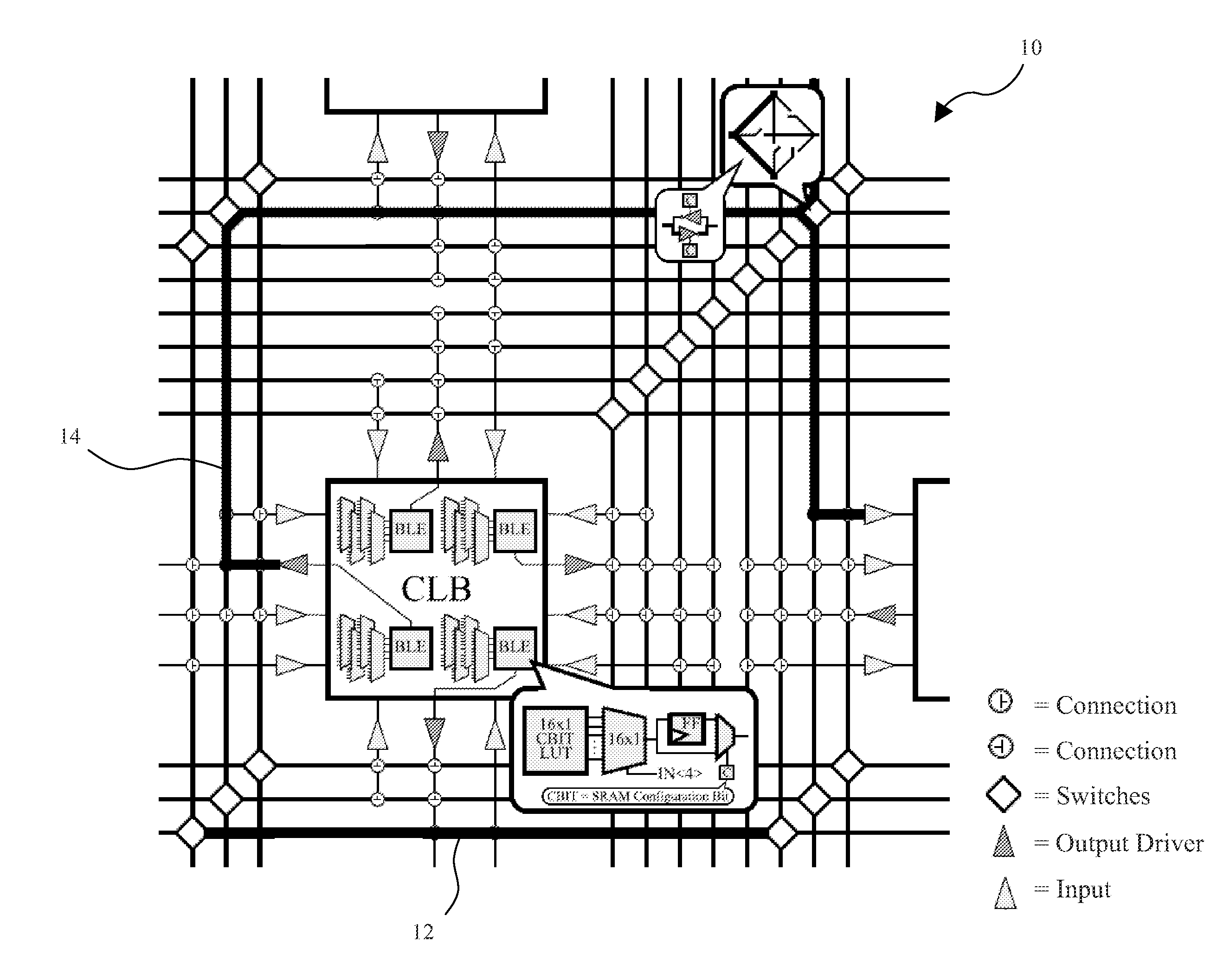
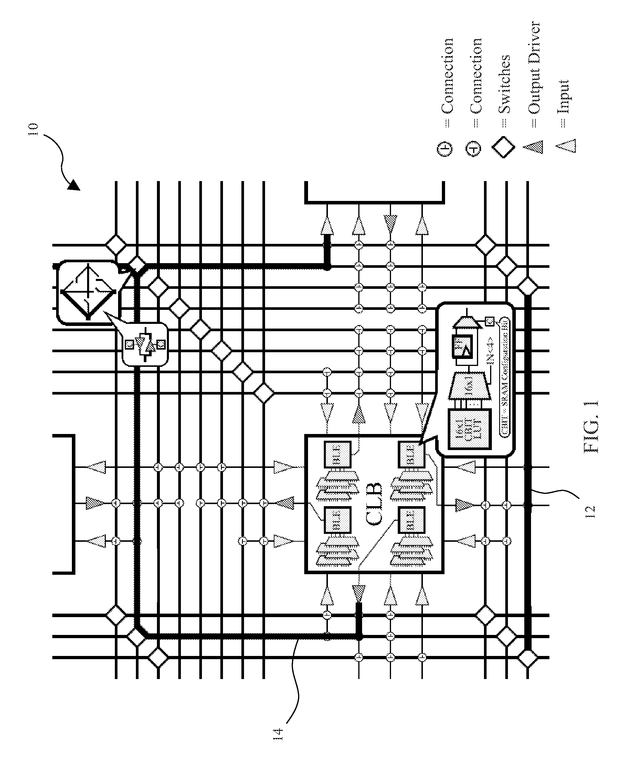
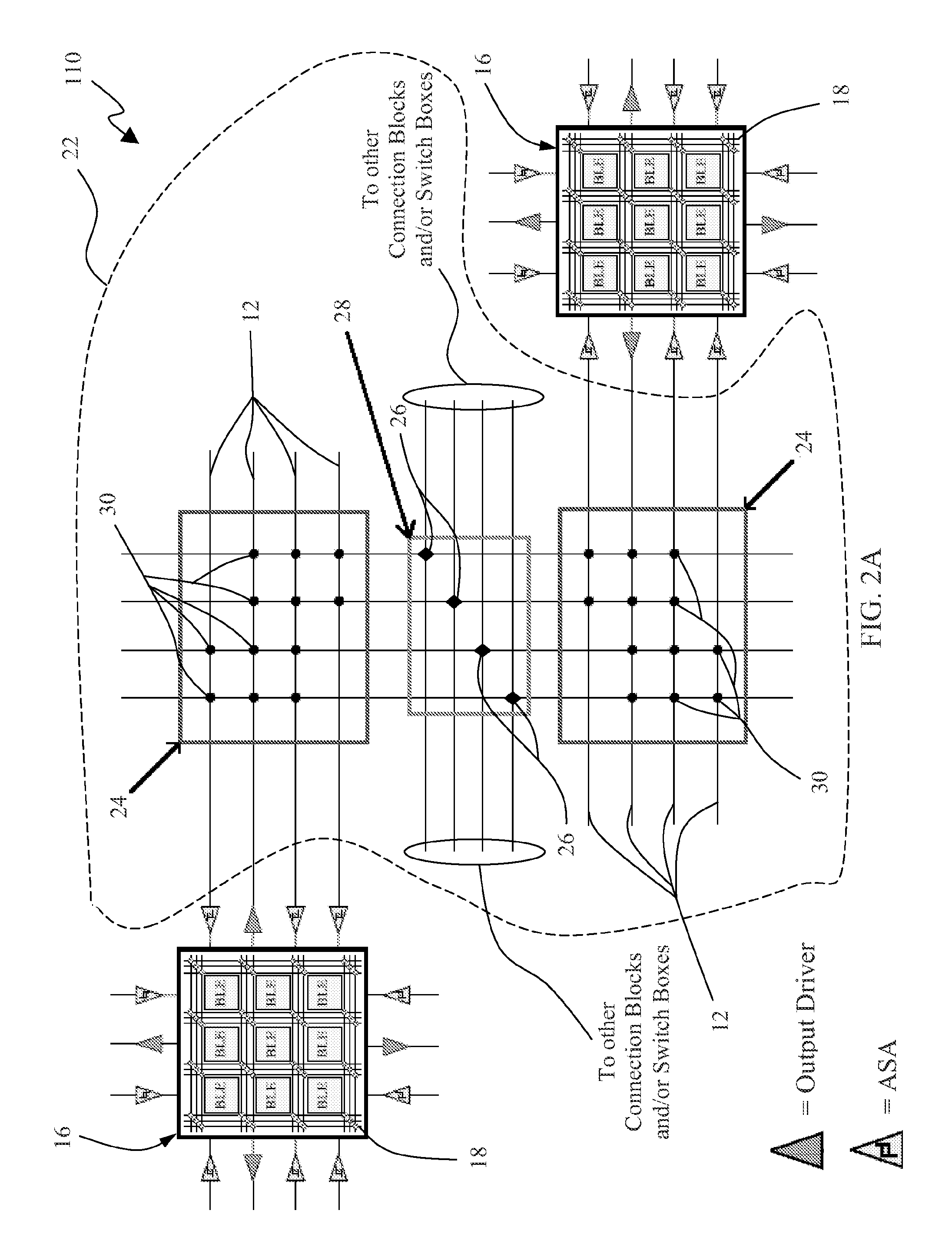
[0052]a plurality of configurable logic blocks (CLBs) for performing combinational and / or sequential logic operations based on programming of the FPGA in response to one or more logic inputs;

[0053]a plurality of programmable routing channels configured for interconnecting the CLBs for routing input signals to the CLBs and output signals from the CLBs based on programming of the FPGA; and

[0054]a plurality of memory cells within the FPGA for configuring logic block operation and signal routing of the programmable routing channels;

[0055]wherein the programmable routing channels comprise:[0056]wire segments surrounding the CLBs;[0057]connection blocks configured for connecting input and output signals of the CLBs with the wire segments;[0058]a pl...

example 43

[0111 may optionally include a method for programming the FPGA of examples 1 or 2 (as well as subject matter of one or more of any combination of examples 1-42).

[0112]Example 44 may optionally include at least in part the method of example 43 (as well as subject matter of one or more of any combination of examples 1-42), wherein the method of programming comprises:

[0113]transforming Verilog or other source code into BLIF;

[0114]performing a placing and routing operation using VPR or a similar tool on the BLIF and architecture components to create a structure;

[0115]analyzing the structure;

[0116]performing timing and energy calculations;

[0117]re-analyzing low-swing and variation aspects of the structure; and

[0118]converting the structure into programming data.

[0119]Example 45 may optionally include at least in part the method of method of example 44 (as well as subject matter of one or more of any combination of examples 1-43), further comprising:

[0120]mapping the output of VPR to a ph...


PUM


Abstract

A sub-VT FPGA uses a low swing, dual-VDD interconnect scheme to reduce FPGA area per LUT, delay at a constant energy, and energy at a constant delay relative to a conventional design at low voltage. These improvements are made possible by a custom asynchronous sense amp, a separated voltage for memory cells, and an improved passgate interconnect to optimize routing delay with low energy overhead. This sub-threshold FPGA design enables energy efficient and cost effective configurable logic for a wide variety of ULP applications.

Description

RELATED APPLICATIONS[0001]This application is a national stage filing of International Application No. PCT / US2011 / 028805 filed on Mar. 17, 2011, which claims priority under 35 U.S.C. §119(e) from U.S. provisional application Ser. No. 61 / 314,870, filed on Mar. 17, 2010, entitled “Flexible Circuits and Architecture for Ultra Low Power and Related Method;” the disclosures of which are incorporated herein by reference in their entirety.GOVERNMENT SUPPORT[0002]This invention was made with Government support under Grant No. W911NF-07-1-0172 awarded by DARPA. The Government has certain rights in this invention.BACKGROUND OF THE INVENTION[0003]Ultra low power (ULP) miniature devices are enabling a new generation of applications for areas such as healthcare and wireless environmental control. Development of these applications is costly, however, as managing strict resource constraints can lead to high design complexity. For example, many require a significant amount of on-chip processing to ...

Claims


Application Information

Patent Timeline
Patent Type & Authority Patents(United States)
IPC IPC(8): H03K19/177
CPCH03K19/17744H03K19/17784H03K19/17788
Inventor CALHOUN, BENTON H.RYAN, JOSEPH F.
Owner UNIV OF VIRGINIA ALUMNI PATENTS FOUND
Why Eureka
Try Eureka