
Micromachined millimeter-wave frequency scanning array

a micro-machined and array technology, applied in the field of micro-machined millimeter-wave frequency scanning arrays, can solve the problems of limiting the scanning speed, requiring several watts of power, and requiring several watts of electronic beam steering radars, so as to reduce the elasticity of parylene, increase the temperature, and increase the bonding time

Active Publication Date: 2016-03-15
RGT UNIV OF MICHIGAN
View PDF5 Cites 7 Cited by
  • Summary
  • Abstract
  • Description
  • Claims
  • Application Information

AI Technical Summary

Benefits of technology

The patent text discusses the use of millimeter-wave (MW) technology for high-speed data transmission and the challenges of measuring absorption on backscattering effects in this region. The text also describes a method for bonding wafers together using a high-quality diffusion barrier layer to prevent degradation of the gold quality during bonding. The resulting structure has a large open area that allows for easy placement of GSG probes. The bond-alignment error is maintained below 5 μm among different samples. Overall, the patent text highlights the technical advantages of MW technology and the importance of precise bonding for high-speed data transmission.

Problems solved by technology

It is especially important to eliminate the use of gimbals because they are slow, bulky and susceptible to mechanical failure and because they experience strong mechanical forces that sharply limit the scanning speed.
On the other hand, electronic beam steering radars are fast but rather expensive and power inefficient, requiring several Watts of power.
In addition, the incorporated phase shifters are bulky and in most cases not available at higher MMW band.
In upper MMW spectrum, excessive conductor loss in the complex feeding networks is a major problem.
However, in these techniques, the height of the waveguide is limited by the maximum thickness of the spun photoresist, limiting the fabrication to the reduced-height waveguides which suffer from high attenuation.
This structure cannot provide broadside radiation without grating lobes.
The scanning range is also limited.
The constructive interference at some other frequencies causes a high reflection.

Method used


Image

  • Micromachined millimeter-wave frequency scanning array
  • Micromachined millimeter-wave frequency scanning array
  • Micromachined millimeter-wave frequency scanning array

Examples


Embodiment Construction

[0078]Example embodiments will now be described more fully with reference to the accompanying drawings.

[0079]Example embodiments are provided so that this disclosure will be thorough, and will fully convey the scope to those who are skilled in the art. Numerous specific details are set forth such as examples of specific components, devices, and methods, to provide a thorough understanding of embodiments of the present disclosure. It will be apparent to those skilled in the art that specific details need not be employed, that example embodiments may be embodied in many different forms and that neither should be construed to limit the scope of the disclosure. In some example embodiments, well-known processes, well-known device structures, and well-known technologies are not described in detail.

[0080]The terminology used herein is for the purpose of describing particular example embodiments only and is not intended to be limiting. As used herein, the singular forms “a,”“an,” and “the” ...


PUM


Abstract

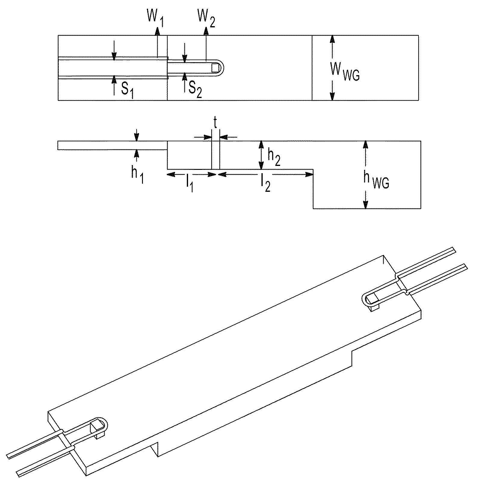
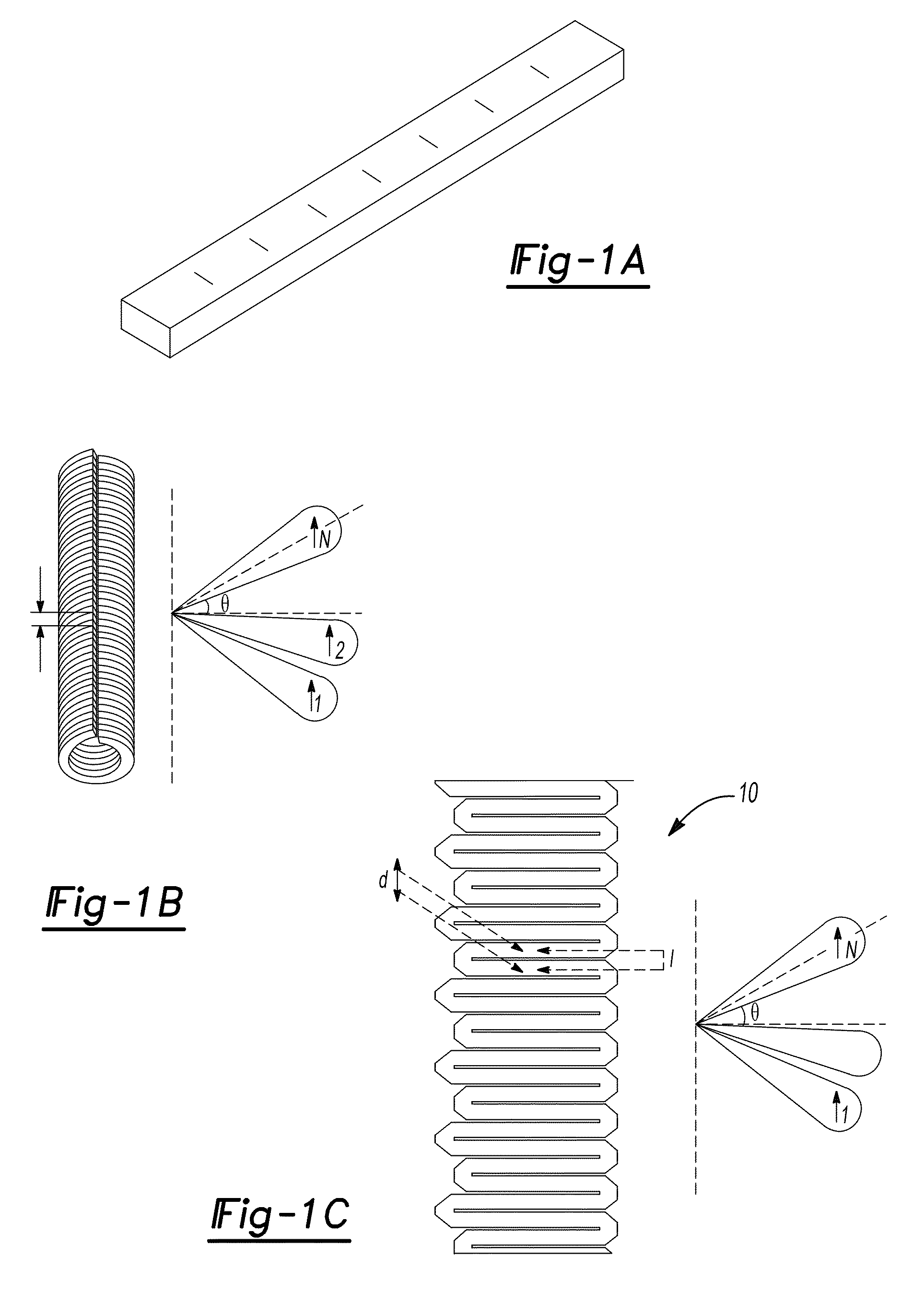
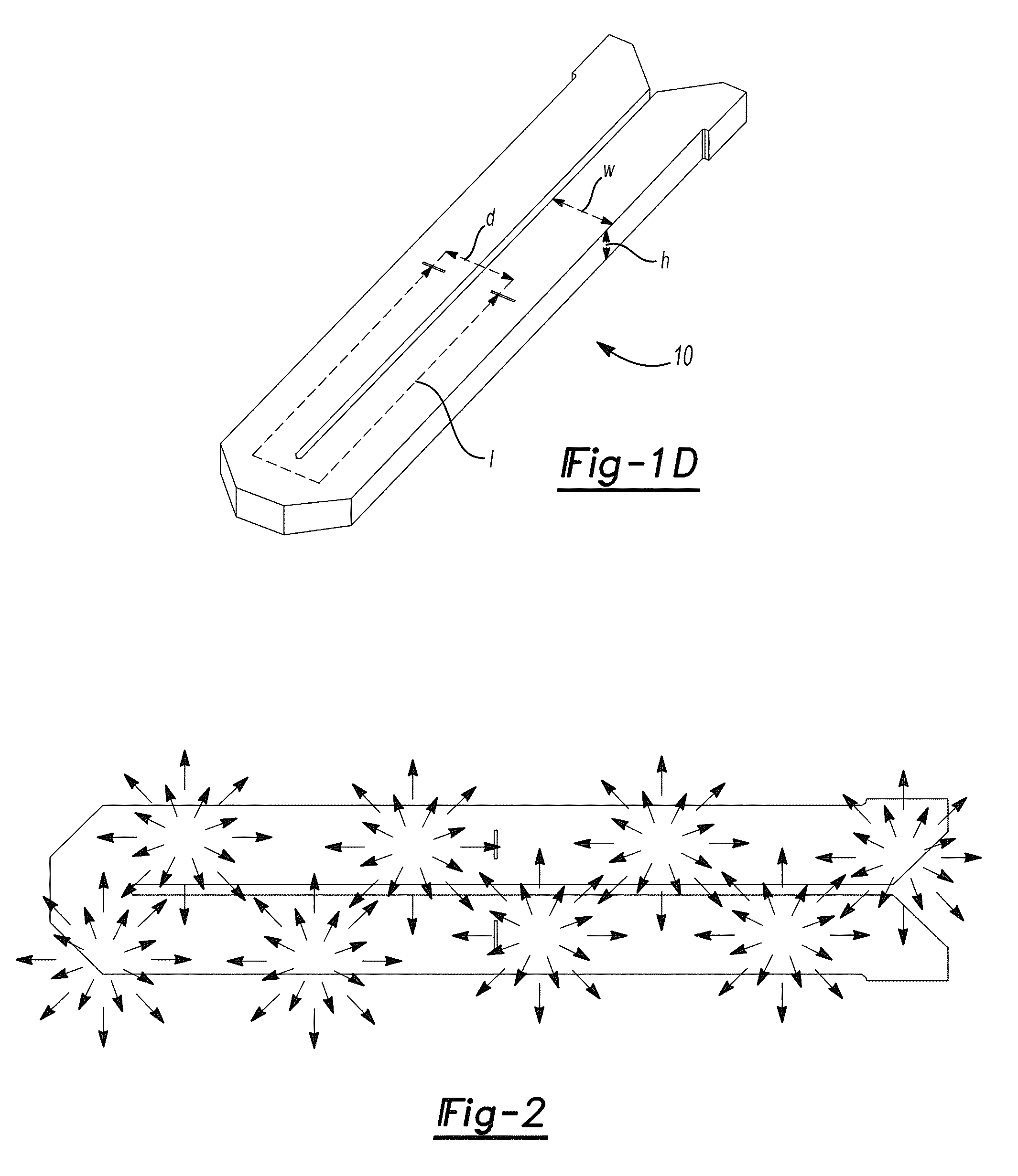
A frequency scanning traveling wave antenna array is presented for Y-band application. This antenna is a fast wave leaky structure based on rectangular waveguides in which slots cut on the broad wall of the waveguide serve as radiating elements. A series of aperture-coupled patch arrays are fed by these slots. This antenna offers 2° and 30° beam widths in azimuth and elevation direction, respectively, and is capable of ±25° beam scanning with frequency around the broadside direction. The waveguide can be fed through a membrane-supported cavity-backed CPW which is the output of a frequency multiplier providing 230˜245 GHz FMCW signal. This structure can be planar and compatible with micromachining application and can be fabricated using DRIE of silicon.

Description

CROSS-REFERENCE TO RELATED APPLICATIONS[0001]This application claims the benefit of U.S. Provisional Application No. 61 / 529,376, filed on Aug. 31, 2011. The entire disclosure of the above application is incorporated herein by reference.GOVERNMENT INTEREST[0002]This invention was made with government support under Grant No. W911 NF-08-2-0004 awarded by the U.S. Army Research Office. The government has certain rights in the invention.FIELD[0003]The present disclosure relates to a micromachined millimeter wave frequency scanning array.BACKGROUND AND SUMMARY[0004]This section provides background information related to the present disclosure which is not necessarily prior art. This section provides a general summary of the disclosure, and is not a comprehensive disclosure of its full scope or all of its features.[0005]Due to the increased potential applications in the areas of wireless communication systems, imaging systems, atmospheric studies, autonomous vehicle control, perimeter secu...

Claims


Application Information

Patent Timeline
Patent Type & Authority Patents(United States)
IPC IPC(8): H01Q13/10H01Q1/36H01Q21/06H01Q21/00H01Q13/20H01Q13/18
CPCH01Q1/36H01Q13/10H01Q13/18H01Q13/203H01Q21/0037H01Q21/065
Inventor VAHIDPOUR, MEHRNOOSHSARABANDI, KAMALEAST, JACKMOALLEM, MEYSAM
Owner RGT UNIV OF MICHIGAN
Learn More