Control method to reduce switching loss on MOSFET

a control method and switching component technology, applied in the direction of electric variable regulation, process and machine control, instruments, etc., can solve the problems of increasing electromagnetic interference (emi), noise and switching commutation problems, corresponding increase in switching and component stress related losses, and relatively high voltage and current stress suffered by the switching components

Active Publication Date: 2016-03-15
FLEXTRONICS AP LLC
View PDF196 Cites 35 Cited by
  • Summary
  • Abstract
  • Description
  • Claims
  • Application Information

AI Technical Summary

Benefits of technology

[0021]In still yet another aspect, another switching mode power converter is disclosed. The power converter includes a transformer, a first switch, a first controller, a diode, a second switch, a second controller, an output capacitor, and a sensing circuit. The transformer has a primary winding coupled to an input supply voltage and a secondary winding. The first switch is coupled in series to the primary winding. The first controller is coupled to the first switch, wherein the first controller is configured to turn the first switch ON and OFF. The diode is coupled in series to the secondary winding. The second switch is coupled in parallel to the diode. The second controller is coupled to the second switch, wherein the second controller is configured to turn the second switch ON and OFF. The output capacitor is coupled to the diode and to the second switch. The sensing circuit is coupled to the secondary winding and to the second controller. The second controller is configured to determine a threshold condition according to data sensed by the sensing circuit and to switch ON the second switch when the threshold condition is achieved thereby forming an alternative current path for a negative secondary current to flow from the output capacitor to the secondary winding. The negative secondary current generates a corresponding discharge current through the primary winding that reduces a voltage across the first switch. The first controller is further configured to determine when the voltage across the first switch drops to a threshold value, and to switch ON the first switch once the voltage drops to the threshold value.

Problems solved by technology

However, an increase in switching frequency can cause a corresponding increase in switching and component stress related losses, as well as increased electromagnetic interference (EMI), noise, and switching commutation problems, due to the rapid ON / OFF switching of the semiconductor switches at high voltage and / or high current levels.
However, in the flyback converter, the primary and secondary windings of the transformer do not carry current simultaneously.
A drawback to use of the flyback is the relatively high voltage and current stress suffered by the switching components.
Additionally, high turn-off voltage (caused by the parasitic oscillation between transformer leakage inductance and switch capacitance) seen by the primary switch traditionally requires the use of a resistor, capacitor, diode subcircuit, such as a snubber circuit.
This parasitic oscillation is extremely rich in harmonics and pollutes the environment with EMI, and causes high switching losses from the switching components in the form of extra thermal dissipation.
However, the complexity required to provide control to the power switches, such as the transistor T1 in FIG. 1, and the components associated with complex controls, create a limited use in commercial applications.
However, energy losses incurred during control of zero voltage switching and / or zero current switching, and losses incurred during driving, and controlling the resonance means, are still problematic.
However, the lower the valley voltage level, the higher the voltage spike across the transistor when the transistor is switched OFF.
However, the resonant current between the transformer and the added capacitor across the freewheeling diode increases the current stress on the secondary winding and leads to additional conductive dissipation.

Method used


Image

  • Control method to reduce switching loss on MOSFET
  • Control method to reduce switching loss on MOSFET
  • Control method to reduce switching loss on MOSFET

Examples


Embodiment Construction

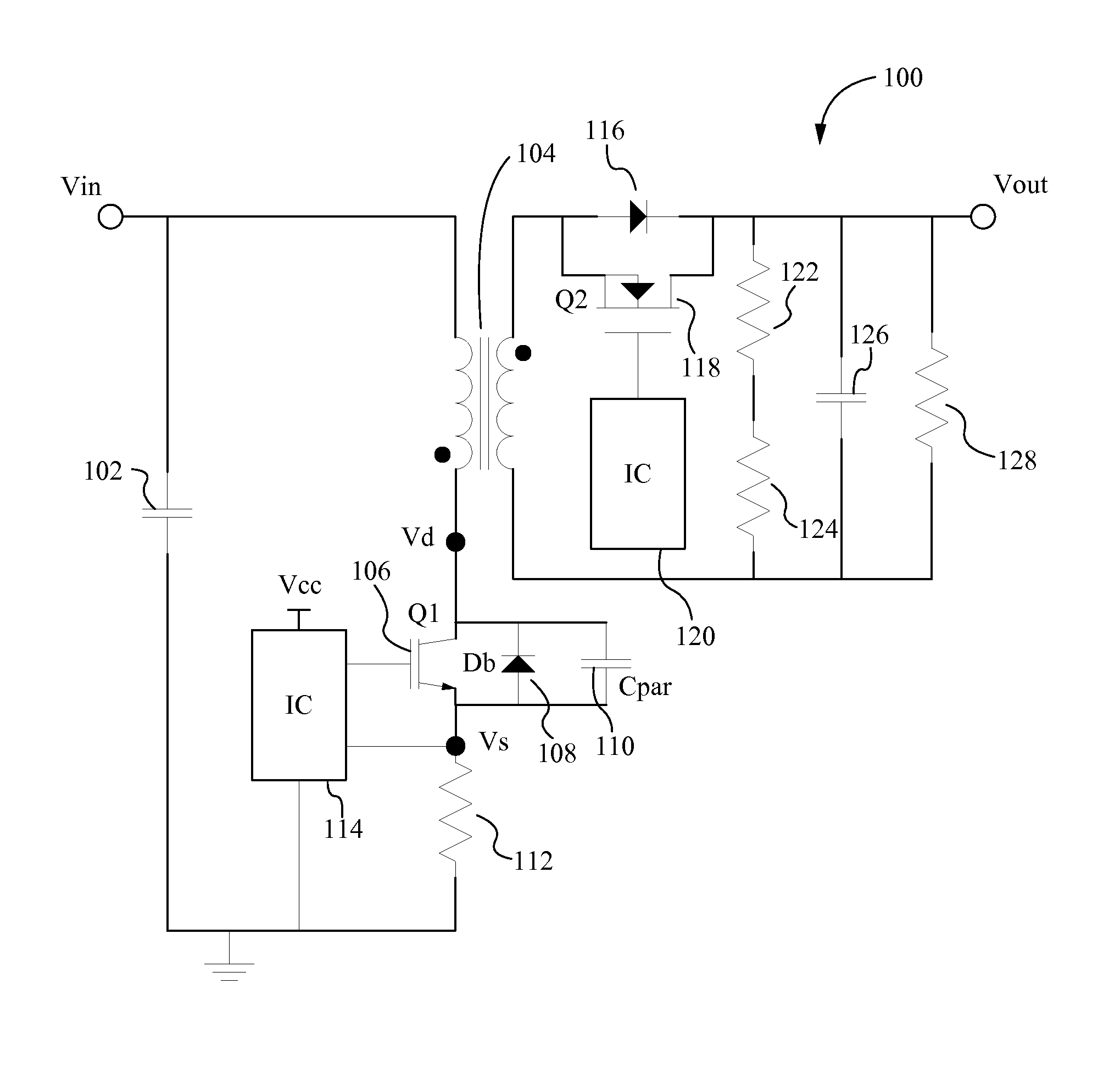
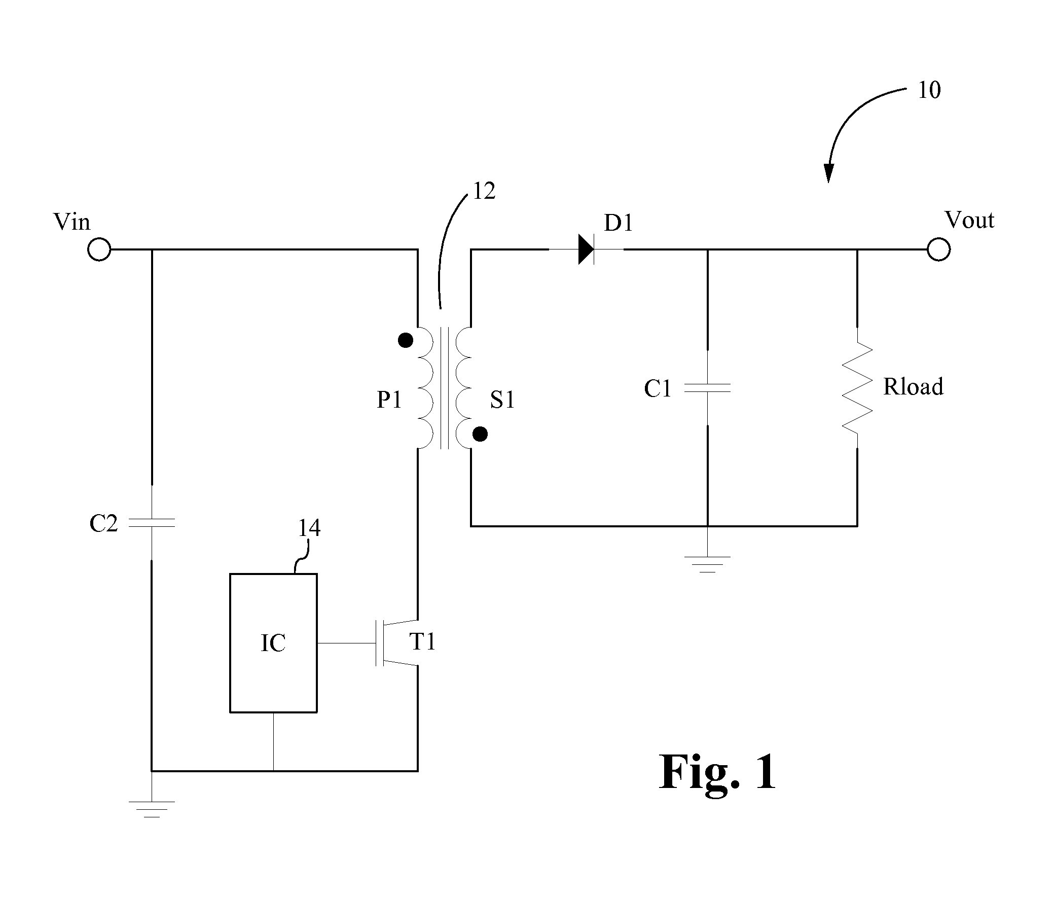
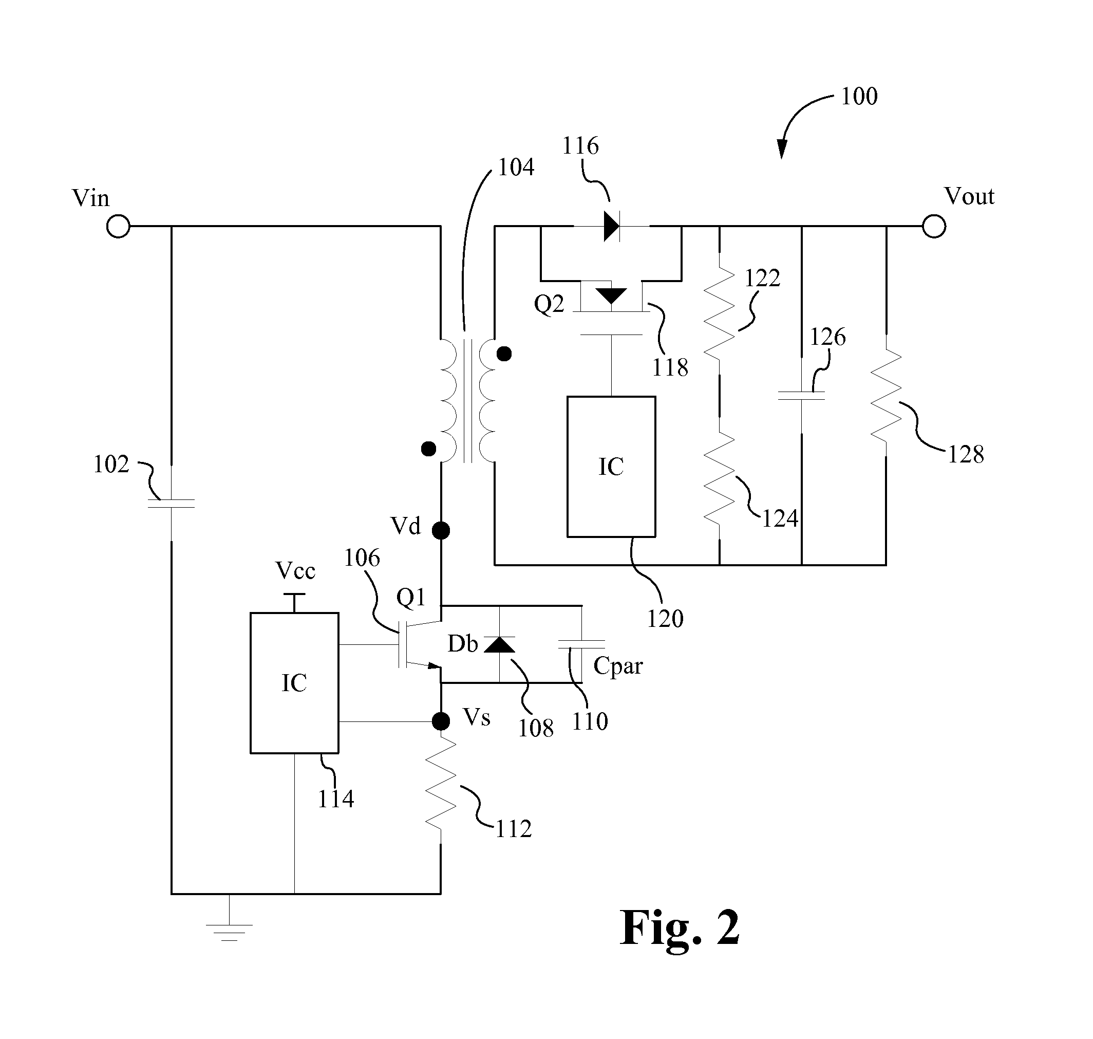
[0026]Embodiments of the present application are directed to a power converter. Those of ordinary skill in the art will realize that the following detailed description of the power converter is illustrative only and is not intended to be in any way limiting. Other embodiments of the power converter will readily suggest themselves to such skilled persons having the benefit of this disclosure.

[0027]Reference will now be made in detail to implementations of the power converter as illustrated in the accompanying drawings. The same reference indicators will be used throughout the drawings and the following detailed description to refer to the same or like parts. In the interest of clarity, not all of the routine features of the implementations described herein are shown and described. It will, of course, be appreciated that in the development of any such actual implementation, numerous implementation-specific decisions must be made in order to achieve the developer's specific goals, such...


PUM


Abstract

A method of controlling a switching mode power converter enables zero voltage switching by forcing a voltage across the main switch to zero. This is accomplished by sensing when a current on the secondary side of the power converter drops to zero, or other threshold value, and then generating a negative current through the secondary winding in response. The negative secondary current results in a corresponding discharge current in the primary winding, which reduces the voltage across the main switch. The voltage across the main switch is monitored such that when the voltage reaches zero, or other threshold value, the main switch is turned ON. In this manner, the circuit functions as a bi-directional current circuit where a forward current delivers energy to a load and a reverse current provides control for reducing the voltage across the main switch to enable zero voltage switching.

Description

FIELD OF THE INVENTION[0001]The present invention is generally directed to the field of power converters. More specifically, the present invention is directed to controlling the switching of a switching device used in a power converter to reduce switching loss.BACKGROUND OF THE INVENTION[0002]There are several power converter topologies that have been developed over the years, which are intended to improve the power density and switching efficiency of power converters. An emerging focus of new converter topologies is to provide a means to reduce or eliminate converter switching losses, while increasing the switching frequencies. Lower loss and higher switching frequency means more efficient converters, which can reduce the size and weight of converter components. Additionally, with the introduction of high speed composite semiconductor switches, such as metal oxide semiconductor field effect transistor (MOSFET) switches operated by pulse width modulation (PWM), recent forward and fl...

Claims


Application Information

Patent Timeline
Patent Type & Authority Patents(United States)
IPC IPC(8): H02M3/335H02M1/00
CPCH02M3/33592H02M3/33576H02M2001/0058Y02B70/1475Y02B70/1491H02M1/0058Y02B70/10
Inventor TELEFUS, MARKLI, WEI
Owner FLEXTRONICS AP LLC
Why Eureka
Try Eureka