LDMOS transistor having elevated field oxide bumps and method of making same

a technology of ldmos transistor and oxide bump, which is applied in the manufacture of transistors, semiconductor/solid-state devices, electrical devices, etc., can solve the problem that the current path through the resulting ldmos transistor is substantially unimpeded by the shallow field oxide region

Active Publication Date: 2016-05-03
TOWER SEMICONDUCTOR
View PDF23 Cites 3 Cited by
  • Summary
  • Abstract
  • Description
  • Claims
  • Application Information

AI Technical Summary

Benefits of technology

[0013]After the shallow field oxide region has been formed, a layer of gate dielectric material may be deposited over the resulting structure, wherein the gate dielectric material covers the hard mask and fills the opening of the hard mask. A chemical mechanical polishing step is then performed to remove the gate dielectric material located over the hard mask. The CMP step is stopped on the upper surface of the hard mask, thereby leaving a gate dielectric region on top of the shallow field oxide region (within the opening of the hard mask). The hard mask is removed and the remainder of the LDMOS transistor is fabricated using conventional CMOS processing steps. The thickness of the gate dielectric region is effectively selected by controlling the height of the hard mask.

Problems solved by technology

As a result, the current path through the resulting LDMOS transistor is substantially unimpeded by the shallow field oxide region.

Method used


Image

  • LDMOS transistor having elevated field oxide bumps and method of making same
  • LDMOS transistor having elevated field oxide bumps and method of making same
  • LDMOS transistor having elevated field oxide bumps and method of making same

Examples


Embodiment Construction

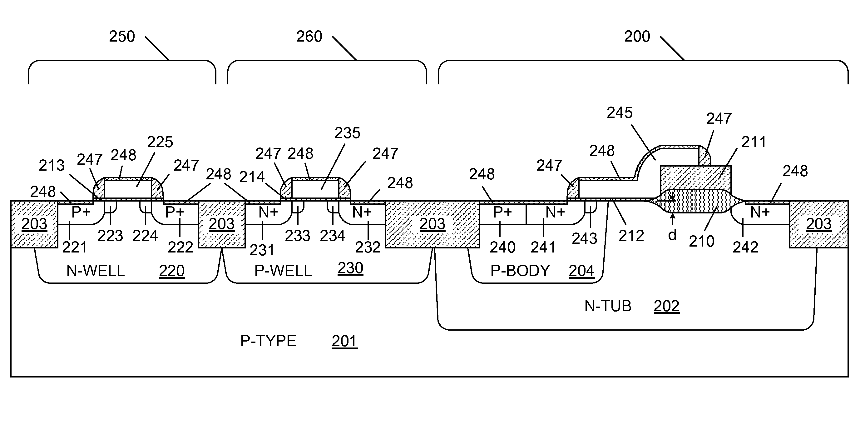
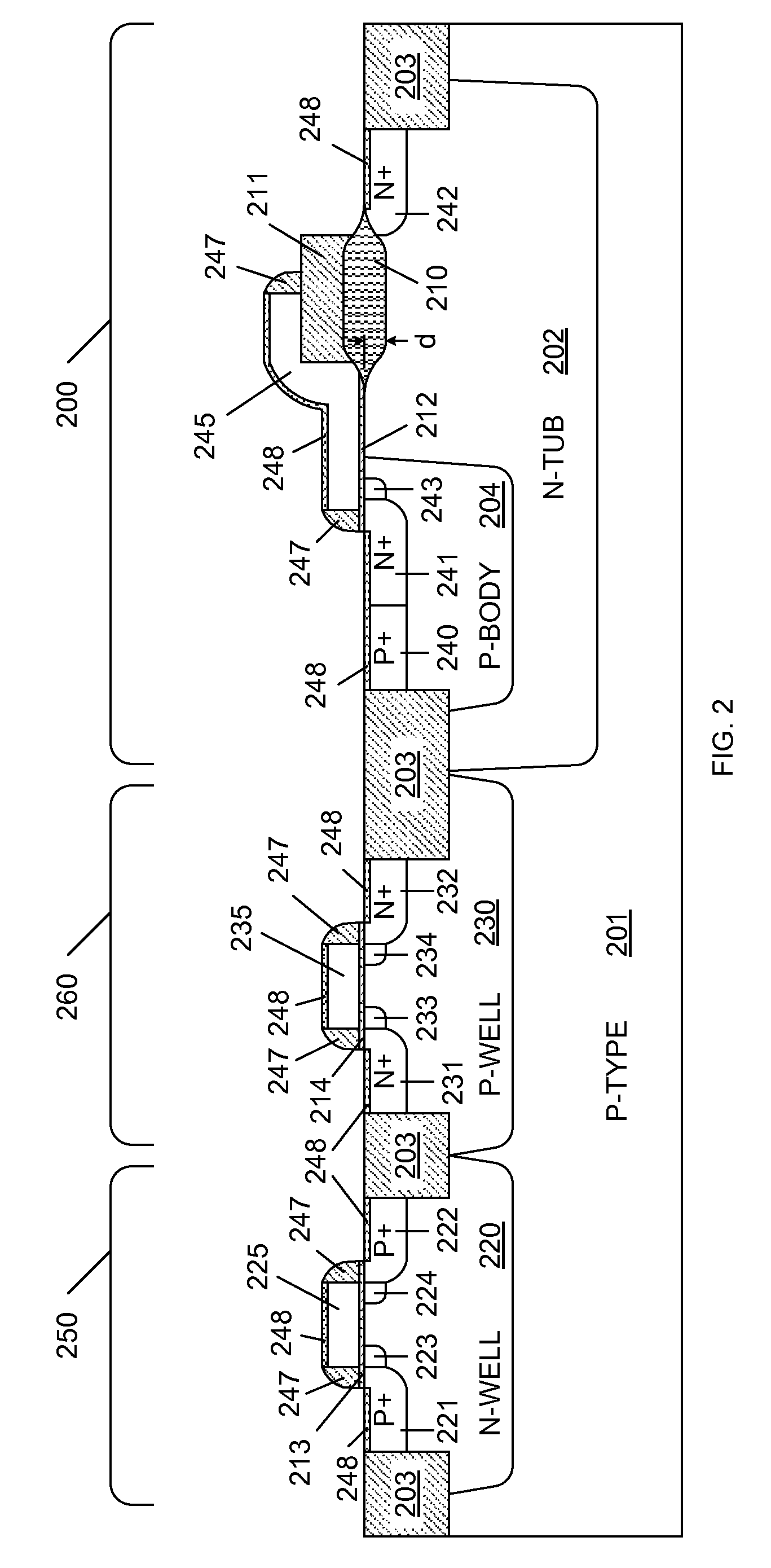
[0023]FIG. 2 is a cross-sectional view of an LDMOS transistor 200 in accordance with one embodiment of the present invention. FIG. 2 also includes cross-sectional views of low voltage MOS transistors 250 and 260, which are fabricated on the same substrate as LDMOS transistor 200. As described in more detail below, the structure of FIG. 2 can be fabricated using a process that is compatible with a conventional deep sub-micron VLSI (CMOS) process. Transistors 200, 250 and 260 (and other circuit elements fabricated on the same substrate) are isolated by field isolation regions 203. In the illustrated embodiments, field isolation regions 203 are shallow trench isolation (STI) regions that extend below the surface of substrate 201 to a depth of about 3500 Angstroms. In alternate embodiments, field isolation regions 203 may be fabricated by LOCOS or PBL techniques, such that these field isolation regions have a birds beak profile and a depth of about 2500 Angstroms.

[0024]LDMOS transistor ...


PUM


Abstract

A low Rdson LDMOS transistor having a shallow field oxide region that separates a gate electrode of the transistor from a drain diffusion region of the transistor. The shallow field oxide region is formed separate from the field isolation regions (e.g., STI regions) used to isolate circuit elements on the substrate. Fabrication of the shallow field oxide region is controlled such that this region extends below the upper surface of the semiconductor substrate to a depth that is much shallower than the depth of field isolation regions. For example, the shallow field oxide region may extend below the upper surface of the substrate by only Angstroms or less. As a result, the current path through the resulting LDMOS transistor is substantially unimpeded by the shallow field oxide region, resulting in a low on-resistance.

Description

RELATED APPLICATION[0001]The present application is related to commonly owned U.S. patent application Ser. No. 11 / 691,459, filed Mar. 26, 2007 and entitled “Self-Aligned LDMOS Fabrication Method Integrated Deep-Sub-Micron VLSI Process, Using A Self-Aligned Lithography Etches And Implant Process”.BACKGROUND OF THE INVENTION[0002]1. Field of the Invention[0003]The present invention relates to a lateral diffused MOSFET (LDMOS) transistor having an elevated gate dielectric structure, which significantly reduces on-resistance (RDSON) while increasing the breakdown voltage and improving the device robustness to hot carrier degradation. The device can be easily integrated with conventional deep sub-micron VLSI processes.[0004]2. Related Art[0005]FIG. 1A is a cross sectional view of a conventional LDMOS transistor 100, which includes P+ substrate 101, P− epitaxial layer 102, deep p-well region 103, P+ backgate contact 104, N+ source region 105, N type reduced surface field region 106, N+ dr...

Claims


Application Information

Patent Timeline
Patent Type & Authority Patents(United States)
IPC IPC(8): H01L21/336H01L29/423H01L29/66H01L21/8238H01L21/8234H01L29/78H01L21/265H01L29/08H01L29/40
CPCH01L21/823462H01L21/823418H01L21/823814H01L21/823857H01L29/42368H01L29/66689H01L29/7816H01L21/26586H01L29/086H01L29/402
Inventor LEVIN, SHARONHEIMAN, ALEXEYSHAKED, ZOHARFLEISHON, GAL
Owner TOWER SEMICONDUCTOR
Why Eureka
Try Eureka