Patterning method

a technology of semiconductors and layers, applied in the field of semiconductor processes, can solve the problems of traditional lithography's limitation on printing small geometry beyond the resolution of photolithography, and the need for thinner photoresist layers, and achieve the effect of reducing device dimensions and effective photoresist thickness

Inactive Publication Date: 2016-07-07
MACRONIX INT CO LTD
View PDF6 Cites 0 Cited by
  • Summary
  • Abstract
  • Description
  • Claims
  • Application Information

AI Technical Summary

Benefits of technology

[0006]The present invention provides a patterning method, in which an etching resistance layer can be provided on an exposed or unexposed photoresist layer, and parts of the etching resistance layer are harden during a baking step to form protection layers respectively on photoresist patterns. By such method, the effective photoresist thickness can be maintained, and the device dimension can be reduced.

Problems solved by technology

However, the photoresist loss is often observed at post exposure baking (PEB), thereby resulting in an undesired thinner photoresist layer.
On the other hand, the traditional lithography has its limitation on printing small geometry beyond the resolution of photolithography.

Method used


Image

  • Patterning method
  • Patterning method
  • Patterning method

Examples


first embodiment

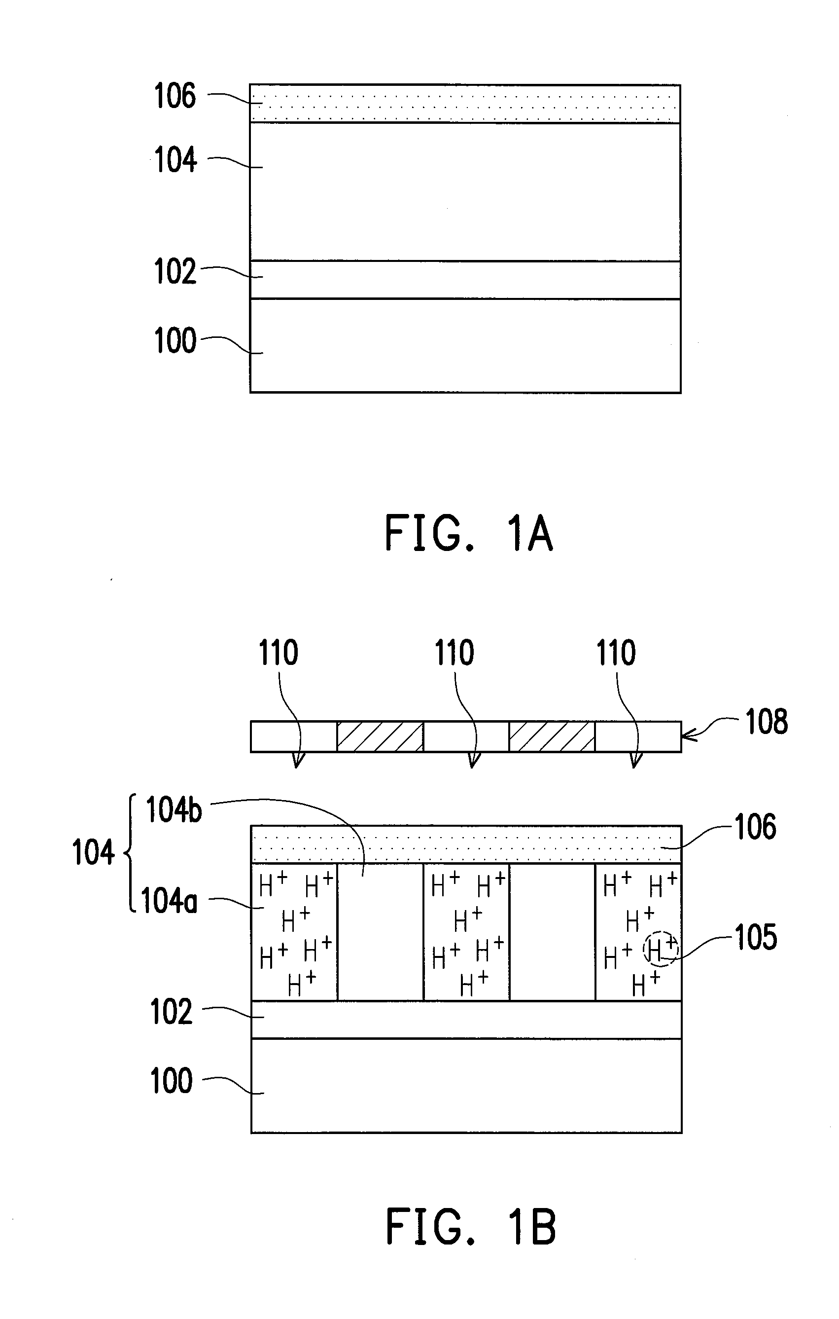
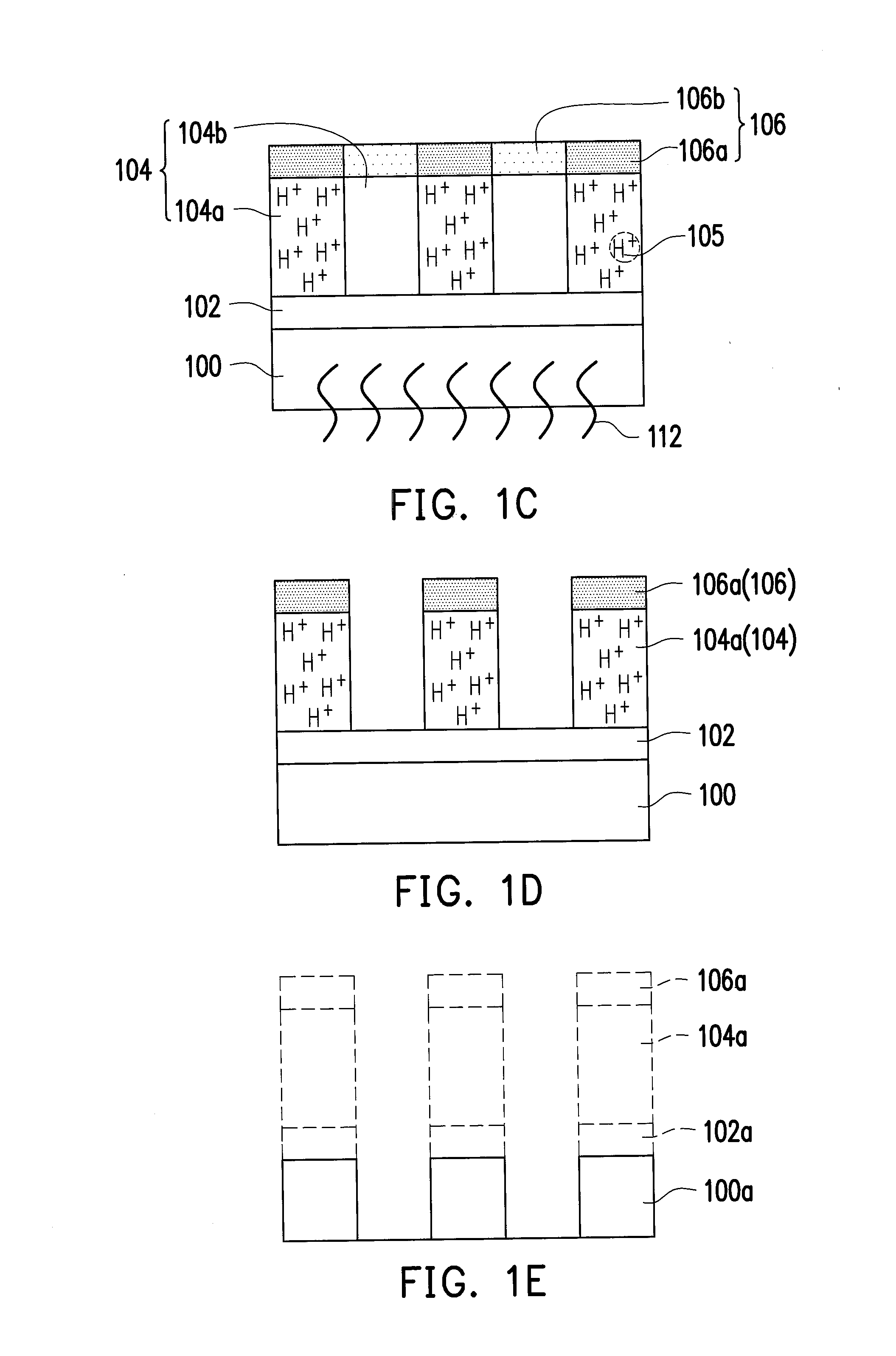
[0033]FIG. 1A to FIG. 1E are schematic cross-sectional views of a patterning method according to a first embodiment of the present invention.

[0034]Referring to FIG. 1A, an optional bottom anti-reflection coating (BARC) layer 102 and a photoresist layer 104 are sequentially formed on a target layer 100. The target layer 100 includes a conductive material, a dielectric material, a semiconductor material or a combination thereof. The BARC layer 102 is configured to reduce the light reflection from the underlying layer(s). The photoresist layer 104 includes a positive photoresist material, such as a 365 nm (I-line) photoresist, a 248 nm (KrF) photoresist, a 193 nm (ArF) photoresist, a immerion-193 nm (immersion-ArF) photoresist or any suitable photoresist. The method of forming each of the BARC layer 102 and the photoresist layer 104 includes performing a spin coating step.

[0035]In an embodiment, the photoresist layer 104 can include a photosensitive resin, a photo-acid generator and a ...

second embodiment

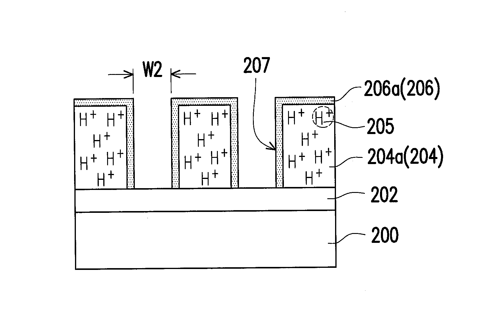
[0044]FIG. 2A to FIG. 2F are schematic cross-sectional views of a patterning method according to a second embodiment of the present invention.

[0045]Referring to FIG. 2A, an optional BARC layer 202 and a photoresist layer 204 are sequentially formed on a target layer 200. The photoresist layer 204 includes a positive photoresist material, such as a 365 nm (I-line) photoresist, a 248 nm (KrF) photoresist, a 193 nm (ArF) photoresist, a immerion-193 nm (immersion-ArF) photoresist or any suitable photoresist. The method of forming each of the BARC layer 202 and the photoresist layer 204 includes performing a spin coating step.

[0046]Referring to FIG. 2B, the photoresist layer 204 is exposed to light 210 through a photomask 208. During the exposing step, a photo acid 205 is generated in first regions 204a of the photoresist layer 204. The photo acid 205 includes a hydrogen ion (H+), for changing the polarity of the exposed first regions 204a. In an embodiment, after the exposing step, the ...


PUM

PropertyMeasurementUnit
etching resistanceaaaaaaaaaa
semiconductoraaaaaaaaaa
feature densityaaaaaaaaaa

Abstract

A patterning method is provided. A photoresist layer is formed on a target layer. An etching resistance layer is formed on the photoresist layer. The photoresist layer is exposed to light and therefore a photo acid is generated in first regions of the photoresist layer. The photoresist layer is developed to remove second regions of the photoresist layer. It is noted that the etching resistance layer is non-photosensitive but reactive to the generated photo acid.

Description

BACKGROUND OF THE INVENTION[0001]1. Field of Invention[0002]The present invention relates to a semiconductor process, and more particularly to a patterning method in a photolithography stage.[0003]2. Description of Related Art[0004]As the level of integration of integrated circuits is getting increased, the demand for increasing the feature density or reducing the pitch size becomes the mainstream in the semiconductor industry, and the key technology is in photolithography. In the photolithography process, a photoresist layer is coated on a wafer. The photoresist layer is exposed to light and therefore a portion thereof is polymerized. The photoresist layer is developed to dissolve the non-polymerized portion thereof. The resulting photoresist layer can be used as an etching mask for the subsequent etching process.[0005]However, the photoresist loss is often observed at post exposure baking (PEB), thereby resulting in an undesired thinner photoresist layer. In such case, the etching...

Claims


Application Information

Patent Timeline
Patent Type & Authority Applications(United States)
IPC IPC(8): H01L21/027G03F7/32G03F7/38G03F7/20
CPCH01L21/0276G03F7/38G03F7/32G03F7/20G03F7/094G03F7/325G03F7/405H01L21/0271H01L21/0273
Inventor LIN, CHIA-HUAYANG, TIEN-CHUHUANG, CHIH-HAO
Owner MACRONIX INT CO LTD
Why Eureka
Try Eureka