Thin film capacitors embedded in polymer dielectric

a polymer dielectric and capacitor technology, applied in the field of thin film capacitors, can solve the problems of affecting yield, adversely affecting the effect of embedded passive devices within substrates, and difficult to isolate the root cause of some failure and attend to the underlying, so as to reduce the size of capacitors

Active Publication Date: 2016-05-24
ZHUHAI ADVANCED CHIP CARRIERS & ELECTRONICS SUBSTRATE SOLUTIONS TECH
View PDF2 Cites 10 Cited by
  • Summary
  • Abstract
  • Description
  • Claims
  • Application Information

AI Technical Summary

Benefits of technology

[0030]The capacitor may be terminated by copper pads separated by solder mask, the copper pads being protected with ENEPIG to prevent tarnish.
[0033]Optionally, the method further comprises an additional step selected from the group consisting of (vb) and (vib) of depositing a layer of aluminium adjacent to the layer of dielectric, and oxidizing to aluminium oxide, thereby sealing defects in the layer of dielectric.
[0035]In some embodiments, subsequent to step (xii) of etching away the seed layer and prior to step (xiv) of lamination, there is an additional step (xiii) of plasma etching the electrodes and the dielectric of the capacitor around the copper via, and reducing the size of the capacitor to the footprint of the copper via thereover.

Problems solved by technology

Embedding passive devices within substrates is not without its downside.
The more complicated the substrate, the higher the likelihood of some aspect failing, and so embedding components can adversely affect yields.
The more complicated and integrated a component, the more difficult it is to isolate a root cause of some failure thereof and to attend to the underlying causes.

Method used


Image

  • Thin film capacitors embedded in polymer dielectric
  • Thin film capacitors embedded in polymer dielectric
  • Thin film capacitors embedded in polymer dielectric

Examples


Embodiment Construction

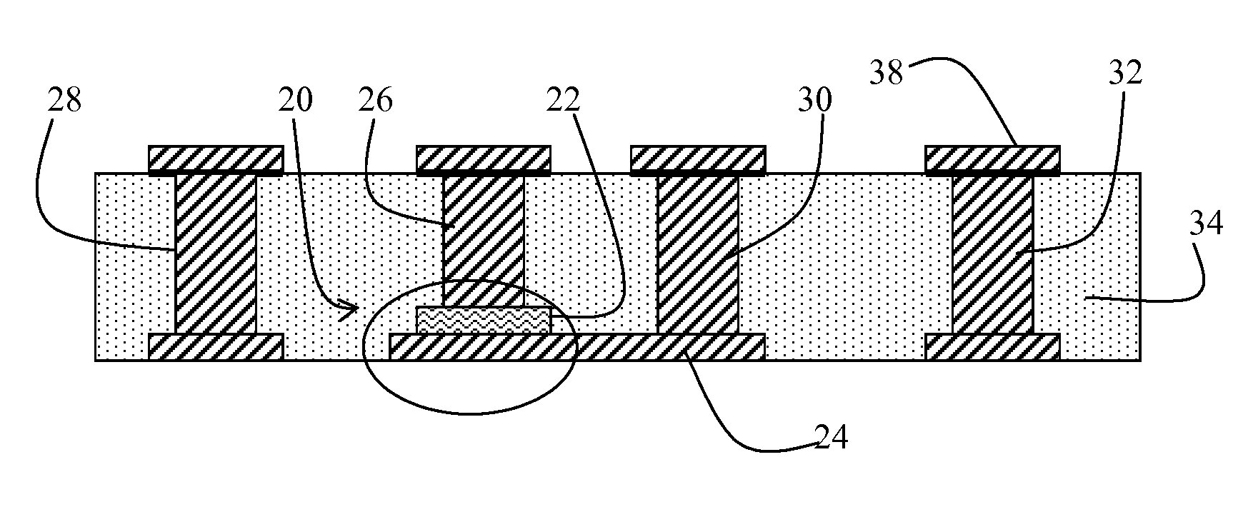
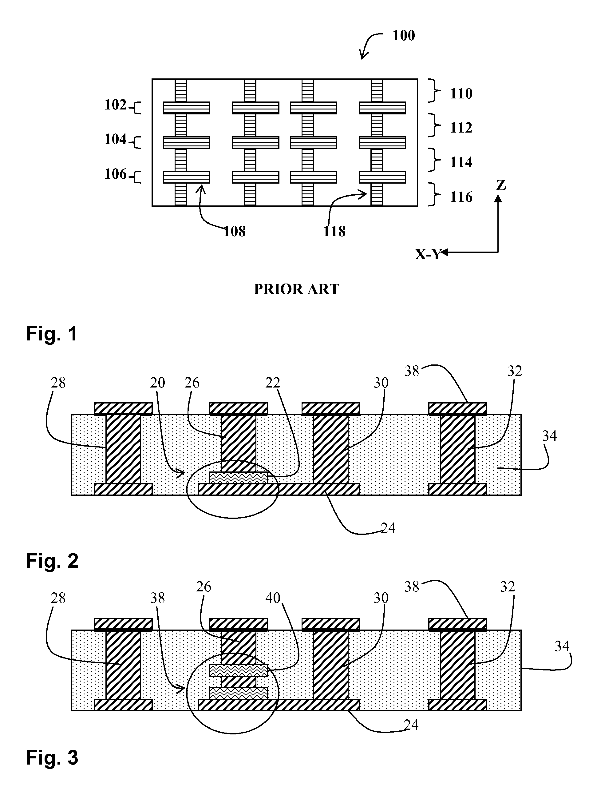
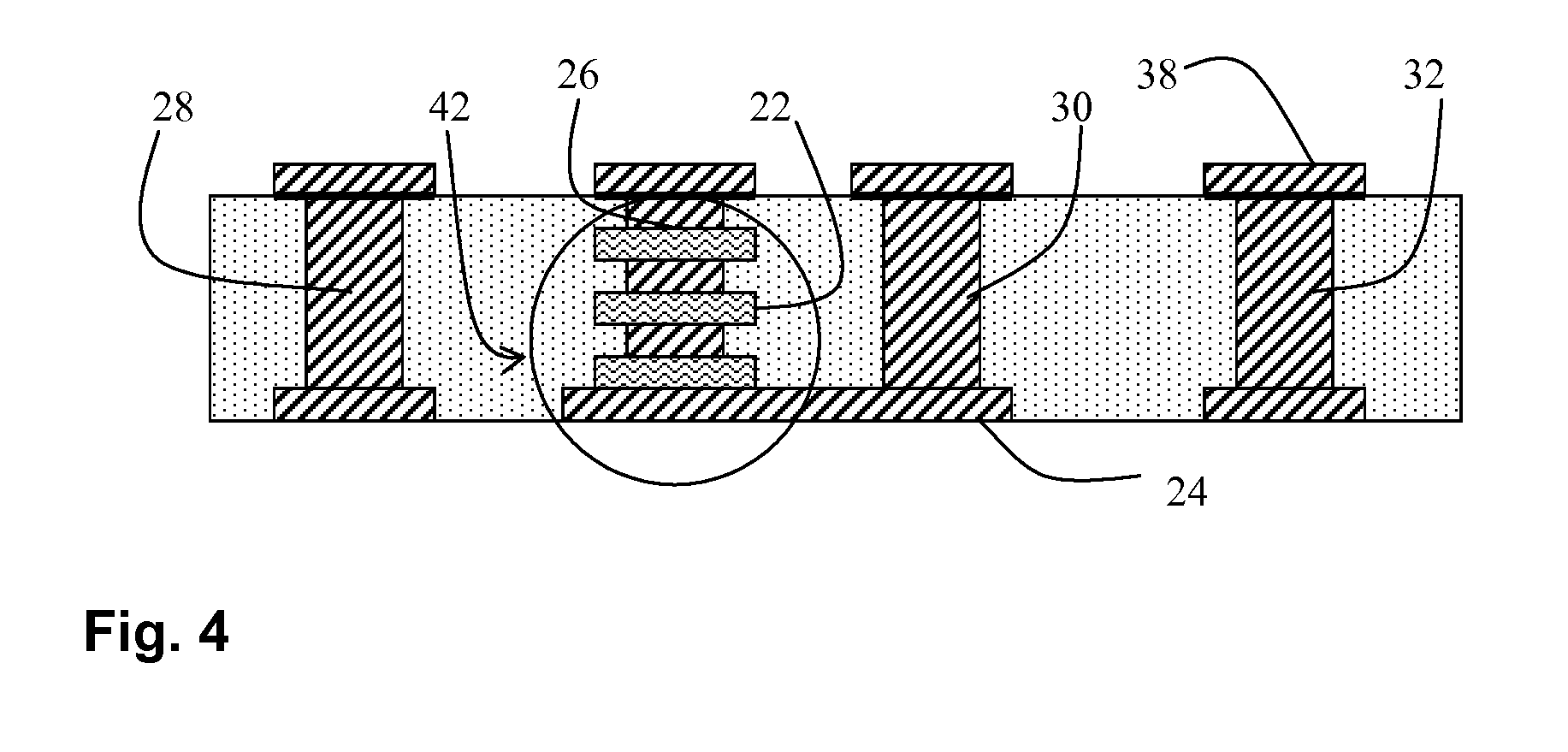
[0061]In the description hereinbelow, support structures consisting of metal vias in a dielectric matrix, particularly, copper via posts in a polymer matrix, such as polyimide, epoxy or BT (Bismaleimide / Triazine) or their blends, reinforced with glass fibers are considered.

[0062]Since capacitors comprise a dielectric material sandwiched between electrodes, typically a material with a very high dielectric constant, the dielectric material used for encapsulation is referred to hereinbelow as an ‘encapsulation dielectric’ or ‘encapsulating dielectric’ to differentiate it from the dielectric of the capacitor.

[0063]It is a feature of Access' photo-resist and pattern or panel plating and laminating technology, as described in U.S. Pat. No. 7,682,972, U.S. Pat. No. 7,669,320 and U.S. Pat. No. 7,635,641 to Hurwitz et al., incorporated herein by reference, that there is no effective upper limit to the in-plane dimensions of a feature.

[0064]FIG. 1 is a simplified section through a multilayer ...


PUM

PropertyMeasurementUnit
mean particle sizeaaaaaaaaaa
diameteraaaaaaaaaa

Abstract

A substrate comprising a capacitor comprising metal electrodes and a ceramic or metal oxide dielectric layer, the capacitor being embedded in a polymer based encapsulating material and connectable to a circuit via a via post standing on said capacitor.

Description

BACKGROUND[0001]1. Field of the Disclosure[0002]The present invention is directed to thin film capacitors, and to multilayer interconnect structures with embedded thin film capacitors.[0003]2. Description of the Related Art[0004]An established method of fabricating electronic substrates and interconnects is by electroplating metal layers and metal interconnects and embedding these in a polymer based dielectric. One fabrication technique uses drill & fill to provide conductive vias.[0005]An alternative solution that overcomes many of the inherent disadvantages of the drill & fill approach, is to fabricate vias by depositing copper or other metal into a pattern created in a photo-resist, using a technology otherwise known as ‘pattern plating’.[0006]In pattern plating, a seed layer is first deposited over a substrate, providing a conducting layer onto which copper may be deposited. Then a layer of photo-resist is deposited thereover and subsequently exposed to create a pattern, and sel...

Claims


Application Information

Patent Timeline
Patent Type & Authority Patents(United States)
IPC IPC(8): H01G4/005H01G4/224H01G4/33H01L49/02H01G4/228
CPCH01L28/65H01G4/224H01G4/228H01G4/33H05K1/162
Inventor HURWITZ, DRORHUANG, ALEX
Owner ZHUHAI ADVANCED CHIP CARRIERS & ELECTRONICS SUBSTRATE SOLUTIONS TECH
Why Eureka
Try Eureka