

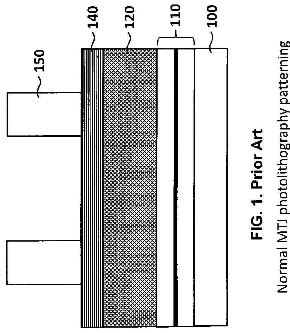
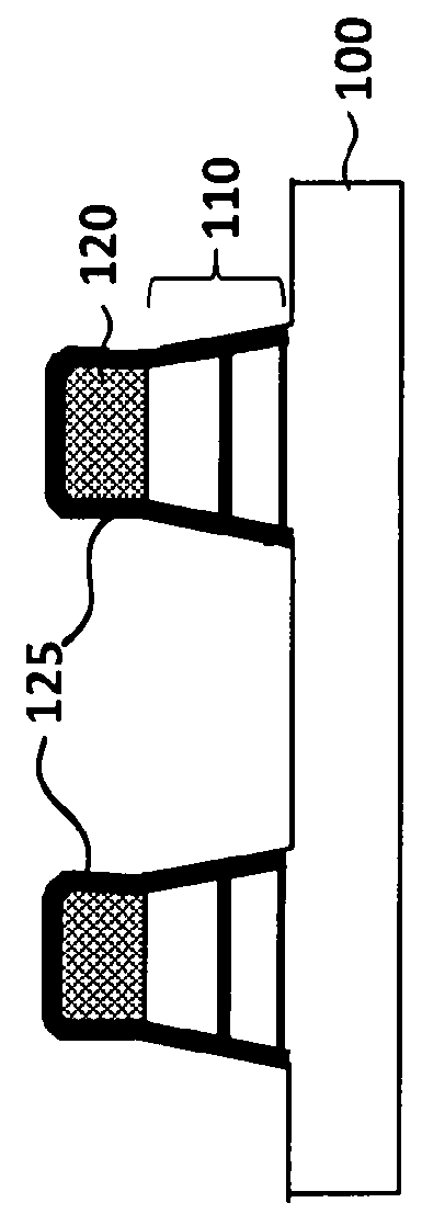
Method of patterning MTJ cell without sidewall damage
- Summary
- Abstract
- Description
- Claims
- Application Information
AI Technical Summary
Benefits of technology
Problems solved by technology
Method used
Image

Examples
first embodiment
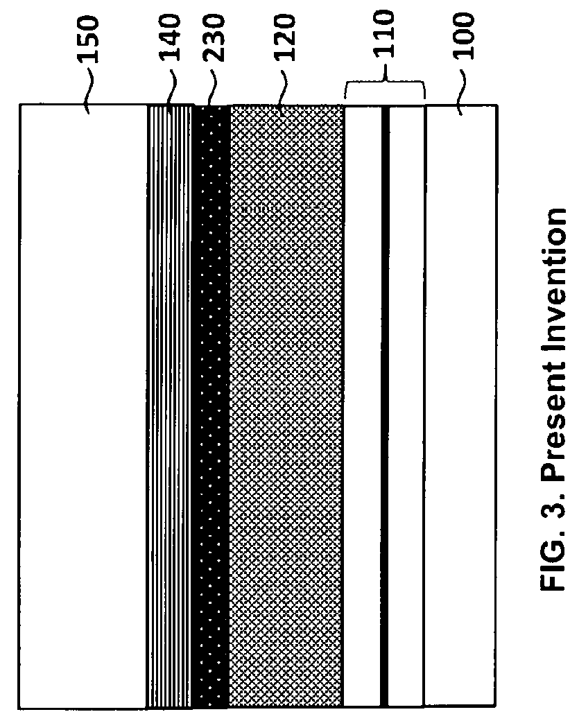
[0056]Illustrated in FIG. 3-FIG. 7, this embodiment starts from having an MRAM film element (MRAM-FE) 110 atop a bottom electrode (BE) base layer 100 made first, wherein a set of required films stacked one by one for forming a functional foundation of MRAM before an MRAM circuit is fabricated. The BE is made of an electric conductor, such as a metal or an alloy. A step forming a hard mask element (HME) 120 / 230 starts with forming a metal Ta layer 120 with a thickness between 40-150 nm followed by forming a carbon layer 230 with a thickness between 20-200 nm atop the Ta layer 120. The Ta layer 120 may be formed by approaches including physical vapor deposition (PVD), or ion-beam deposition (IBD) using Ta as a target. The carbon layer 230 is formed by approaches including one or more of the following methods a). chemical vapor deposition (CVD) using reactants comprising C, H, and O; b). a spin-on-Carbon coating; c). PVD using carbon as a target; and d). IBD using carbon as a target. T...
second embodiment
[0060]As another example, alternatively illustrating the method in present invention, as shown in FIG. 11-FIG. 16, an MRAM film element (MRAM-FE) 110 atop the BE 100 is made first, wherein a set of required films stacked one by one for forming a functional foundation of MRAM before an MRAM circuit is fabricated. A step forming a hard mask element (HME) starts with forming a metal Ta layer 120 with a preferred thickness between 40-150 nm. The next step is forming an etching enhancement layer (EEL) 335 made of one or more of Si oxide (SiO2), Si nitride (SiN), Si oxynitride (SiON), and Si carbide (SiC), atop the carbon layer 230, with a preferred thickness of 50-200 nm. The SiO2 layer of the EEL 335 in HME is formed by approaches including one or more of the following: a). CVD using reactants comprising Si, H, and O; b). spin-on-SiO coating; c). PVD using Si or SiO2 as a target with Ar or Ar+O2 gas(es); and d). IBD using SiO2 as a target. The SiN layer of the EEL 335 in the HME is form...
third embodiment
[0066]As another example, alternatively illustrating the method in present invention, as shown in FIG. 24-FIG. 29, an MRAM film element (MRAM-FE) 110 atop the BE 100 is made first, wherein a set of required films stacked one by one for forming a functional foundation of MRAM before an MRAM circuit is fabricated. A step forming a hard mask element (HME) starts with forming a metal Ta layer 120 with a preferred thickness between 50-150 nm followed by forming a carbon 230 with a preferred thickness between 20-200 nm atop the Ta layer 120, that is formed by approaches including PVD, or IBD using C as a target. The next step is forming an etching enhancement layer (EEL) 335 made of one or more of Si oxide (SiO2), Si nitride (SiN), Si oxynitride (SiON), and Si carbide (SiC), atop the carbon layer 230, with a preferred thickness of 40-200 nm. The SiO2 layer of the EEL 335 in HME is formed by approaches including one or more of the following: a). PECVD using reactants comprising Si, H, and ...
PUM
 Abstract
Description
Claims
Application Information