Enhancement mode high electron mobility transistor

a high electron mobility, transistor technology, applied in the direction of basic electric elements, semiconductor devices, electrical equipment, etc., can solve the problems of limiting the maximum saturated output current of the hemt, difficult control of the threshold voltage of the enhancement mode hemt, complex doping process, etc., to facilitate the control of the hemt, improve the breakdown voltage, and prevent damage

Inactive Publication Date: 2016-08-30
UNIV OF ELECTRONICS SCI & TECH OF CHINA
View PDF3 Cites 10 Cited by
  • Summary
  • Abstract
  • Description
  • Claims
  • Application Information

AI Technical Summary

Benefits of technology

[0012]Specifically, the invention provides a bidirectionally polarized enhancement mode HEMT, which fully utilizes the features of the GaN-based material, including high critical breakdown electric field and high saturated electron velocity, to improve the breakdown voltage of the HEMT. Inversed polarization layers are arranged on the upper surfaces of the barrier layers between the gate electrodes and the drain electrodes, respectively. Inversed polarization is produced by inversed polarization layers and the barrier layers and the 2DHG is formed at the interfaces therebetween. In addition, the metal gate electrode is not disposed between the source electrode and the gate electrode but forms the insulating gate electrode at edges of the source electrodes away from the drain electrodes by the etched groove. In one respect, the longitudinal conductive channels between the source electrodes and the 2DEG are blocked by the corresponding 2DHG, and the electric field of the conductive channel can be controlled by exerting a voltage on the groove-type gate electrode, thereby realizing the enhancement mode and regulating the threshold voltage by doping the conductive channel. In the other respect, the polarization super junction is formed by 2DHG and 2DEG between the source electrode and the drain electrode, which is able to realize the assisted-depletion of the drift region in a blocking state, optimize the horizontal electric field of the HEMT, and improve the voltage resistant performance of the HEMT. In the meanwhile, the preparation process of the HEMT of the invention is compatible with the conventional process, thus establishing an excellent basis for the GaN power integration technology.
[0025]1. In general, the 2DEG produced by polarization enables the AlGaN / GaN material system to have a normally-open channel, while the invention adopts inversed polarization, the highly concentrated 2DHG constitutes the potential barrier of electrons to realize a normally-off channel, which facilitates the control of the HEMT.
[0026]2. To fully utilizing the feature of high critical breakdown electric field of GaN material, the invention employs the inversed polarization layers / the barrier layers / the buffer layer to constitute a bidirectional polarization (super junction) structure, so that the 2DHG assisted depletion of the drift region is achieved in the blocking state, thereby greatly improving the breakdown voltage.
[0027]3. The gate electrode is disposed close to the source electrodes and away from the drain electrodes. Since the gate electrode is in the vicinity of the source electrodes, the gate electrode is prevented from being damaged by the high electric field, thus concentrating the effective area of the HEMT.

Problems solved by technology

However, the doping process thereof is complex.
However, the threshold voltage of the enhancement mode HEMT is difficult to control, and the produced tunneling current limits the maximum saturated output current of the HEMT.
However, the introduction of the field plate increases the parasitic capacitance of the HEMT, which adversely affects the high frequency and switching properties thereof.
However, the fluoride ions treatment induces damage to the AlGaN / GaN heterojunction; moreover, the distribution of the fluoride ions in the thin barrier layer is difficult to control.
However, when the gate voltage is large, leakage current is produced in the gate electrode, which limits the gate voltage swing.

Method used


Image

  • Enhancement mode high electron mobility transistor
  • Enhancement mode high electron mobility transistor
  • Enhancement mode high electron mobility transistor

Examples


example 1

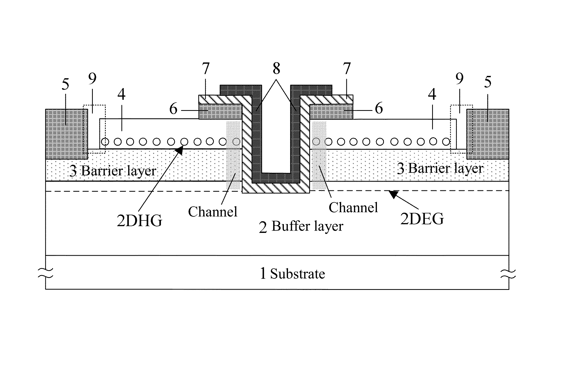
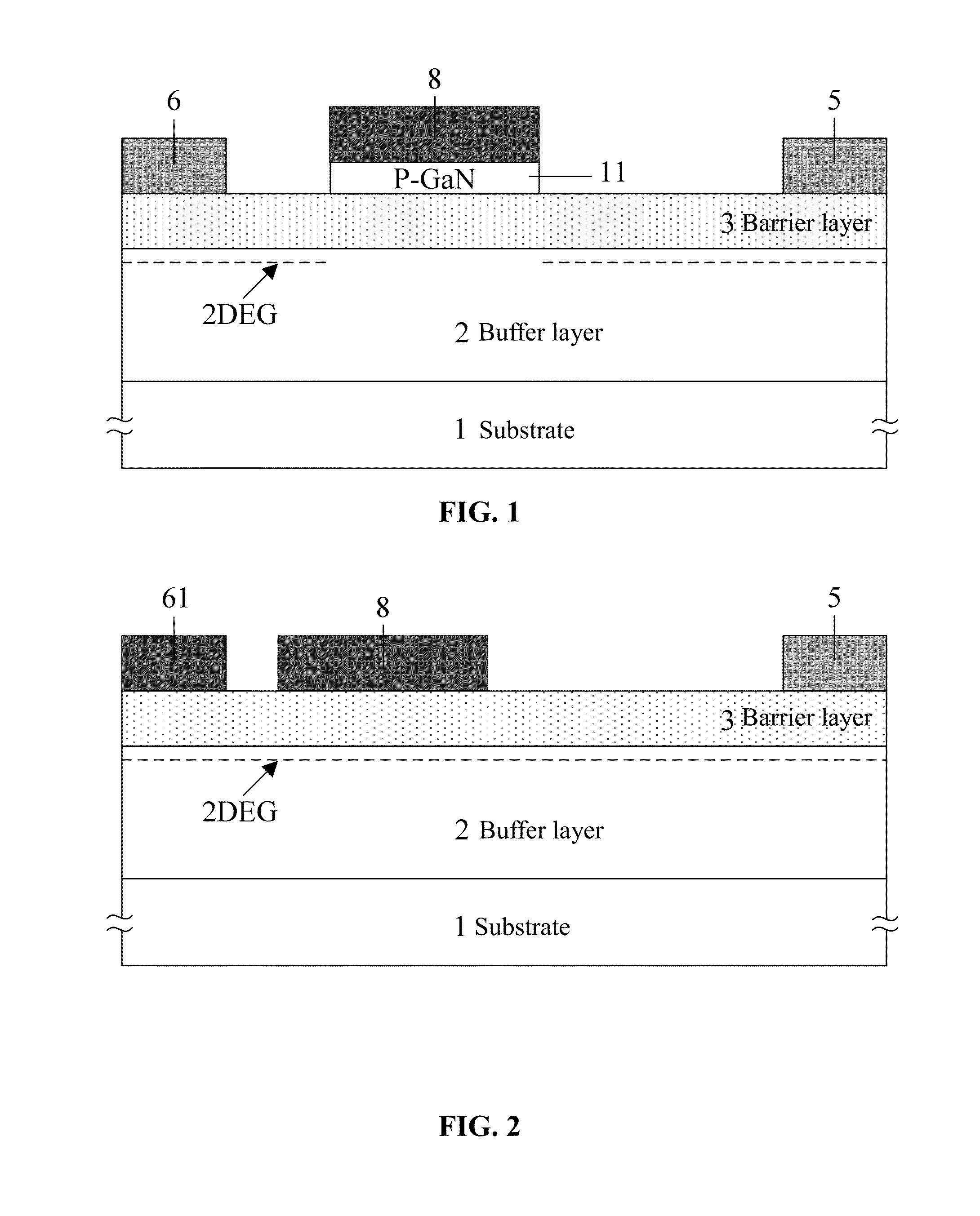
[0041]As shown in FIG. 5, an enhancement mode HEMT comprises: a substrate layer 1, a buffer layer 2 disposed on the substrate layer 1, and barrier layers 3 disposed on the buffer layer 2. An interface between the buffer layer 2 and each barrier layer 3 is provided with a first heterojunction comprising a 2DEG channel. Drain electrodes 5 are disposed at one end of upper surfaces of the barrier layers 3 and form Ohmic contact with the barrier layers 3. Reverse polarization semiconductor layers 4 are disposed on the upper surfaces of the barrier layers 3 and are able to produce inversed polarization with the barrier layers 3. A second heterojunction comprising a 2DHG is formed at an interface between each reverse polarization semiconductor layer 4 and each barrier layer 3. Source electrodes 6 are disposed at one end of upper surfaces of the reverse polarization semiconductor layers 4 away from the drain electrodes 5. Potential wells are formed at connecting interfaces between source el...

example 2

[0043]An enhancement mode HEMT of this example adopts polarized super junction tunneling structure and the hole blocking regions formed by ion implantation. Different from Example 1, the HEMT of this example adopts highly concentrated N-type ion implantation to realize the hole blocking regions 9 between the reverse polarization semiconductor layers 4 and the drain electrodes 5, so that the formation of hole conductive channels are prevented between the source electrodes and the drain electrodes. In addition, P-type doping regions are formed in one part of the reverse polarization semiconductor layers 4 between the drain electrodes and the source electrodes, so as to prevent the electron leakage from the source electrodes to the drain electrodes. Other structures are the same as those of example 1, as shown in FIG. 6. NP junctions formed between the drain electrodes and the source electrodes also function in supporting and voltage-resistance in the blocking state. The isolation mode...

example 3

[0044]The enhancement mode HEMT of this example adopts N-type doping in one part of the reverse polarization semiconductor layers 4 beneath the source electrodes. Compared with Example 1, one part of the reverse polarization semiconductor layers 4 beneath the corresponding source electrodes adopt the N-type doping, while other structures are the same as Example 1, as shown in FIG. 7. In one respect, the N-type doped parts beneath the source electrodes are able to form Ohmic contact between the metals of the source electrodes and the inverted polarization semiconductor layers. In the other respect, the N-type doping is able to regulate the concentration of the 2DHG so as to further regulate a threshold voltage. Other parts of the reverse polarization semiconductor layers 4 can be step doped or linearly doped, so that the horizontal electric field distribution of the drift region of the HEMT is further optimized and the voltage resistance is improved.


PUM


Abstract

An enhancement mode HEMT, including: a substrate layer; a buffer layer; barrier layers; drain electrodes; reverse polarization semiconductor layers; source electrodes; an insulated gate dielectric; and a metal gate electrode The buffer layer is disposed on the substrate layer, and the barrier layers are disposed on the buffer layer. Interfaces between the buffer layer and the barrier layers are provided with first heterojunctions having a two-dimensional electron gas (2DEG) channel. The drain electrodes are disposed at one end of the upper surfaces of the barrier layers and form Ohmic contact with the barrier layers. The reverse polarization semiconductor layers are disposed on the upper surfaces of the barrier layers and are able to produce inversed polarization with the barrier layers. The interfaces between reverse polarization semiconductor layers and barrier layers are provided with second heterojunctions having two-dimensional hole gas (2DHG).

Description

CROSS-REFERENCE TO RELAYED APPLICATIONS[0001]Pursuant to 35 U.S.C. §119 and the Paris Convention Treaty, this application claims the benefit of Chinese Patent Application No. 201510456018.7 filed Jul. 29, 2015, the contents of which are incorporated herein by reference. Inquiries from the public to applicants or assignees concerning this document or the related applications should be directed to: Matthias Scholl P. C., Attn.: Dr. Matthias Scholl Esq., 245 First Street, 18th Floor, Cambridge, Mass. 02142.BACKGROUND OF THE INVENTION[0002]1. Field of the Invention[0003]The invention relates to an enhancement mode high electron mobility transistor (HEMT).[0004]2. Description of the Related Art[0005]For AlGaN / GaN HEMTs, it is well-known that enhancement mode (normally off) HEMTs are superior to depletion mode (normally open) HEMTs.[0006]FIG. 1 shows an enhancement mode AlGaN / GaN HEMT including a P-type GaN-doped gate electrode 11. However, the doping process thereof is complex.[0007]FIG....

Claims


Application Information

Patent Timeline
Patent Type & Authority Patents(United States)
IPC IPC(8): H01L29/20H01L29/205H01L29/778
CPCH01L29/7784H01L29/2003H01L29/205H01L29/1025H01L29/778H01L29/41775H01L29/4236H01L29/7786H01L29/0646H01L29/0653H01L29/0847
Inventor LUO, XIAORONGXIONG, JIAYUNYANG, CHAOWEI, JIEWU, JUNFENGPENG, FUZHANG, BO
Owner UNIV OF ELECTRONICS SCI & TECH OF CHINA
Why Eureka
Try Eureka