
Optical waveguide element and optical modulator

a technology of optical modulator and waveguide element, which is applied in the direction of optical waveguide light guide, optical light guide, instruments, etc., can solve the problems of increasing bit error rate, increasing optical loss, and not being able to realize low optical loss, and achieve high q value in phase modulation, low optical loss, and high extinction ratio in intensity modulation

Active Publication Date: 2016-09-20
THE FUJIKURA CABLE WORKS LTD
View PDF10 Cites 19 Cited by
  • Summary
  • Abstract
  • Description
  • Claims
  • Application Information

AI Technical Summary

Benefits of technology

The present invention provides an optical waveguide element that is suitable for optical integrated circuits, and has high-speed, low optical loss, and a high extinction ratio in intensity modulation or a high Q value in phase modulation.

Problems solved by technology

However, if a silicon waveguide with the width and thickness of a core of submicron scale is used, optical loss is increased due to optical scattering caused by lateral roughness of the waveguide core, and it is not possible to realize low optical loss, which is required for an optical integrated circuit for long-distance wavelength multiplex optical fiber communication.
As a result, if a higher order mode component is superimposed on an intensity modulation signal or a phase modulation signal, an extinction ratio in intensity modulation or a Q value (Q-factor) in phase modulation is decreased, a bit error rate is increased, and an excellent optical communication system is not constructed.
Therefore, it is not possible to realize low optical loss which is required for optical components for long-distance wavelength multiplex optical fiber communication.

Method used


Image

  • Optical waveguide element and optical modulator
  • Optical waveguide element and optical modulator
  • Optical waveguide element and optical modulator

Examples


examples

[0105]Hereinafter, the present invention will be specifically described based on examples.

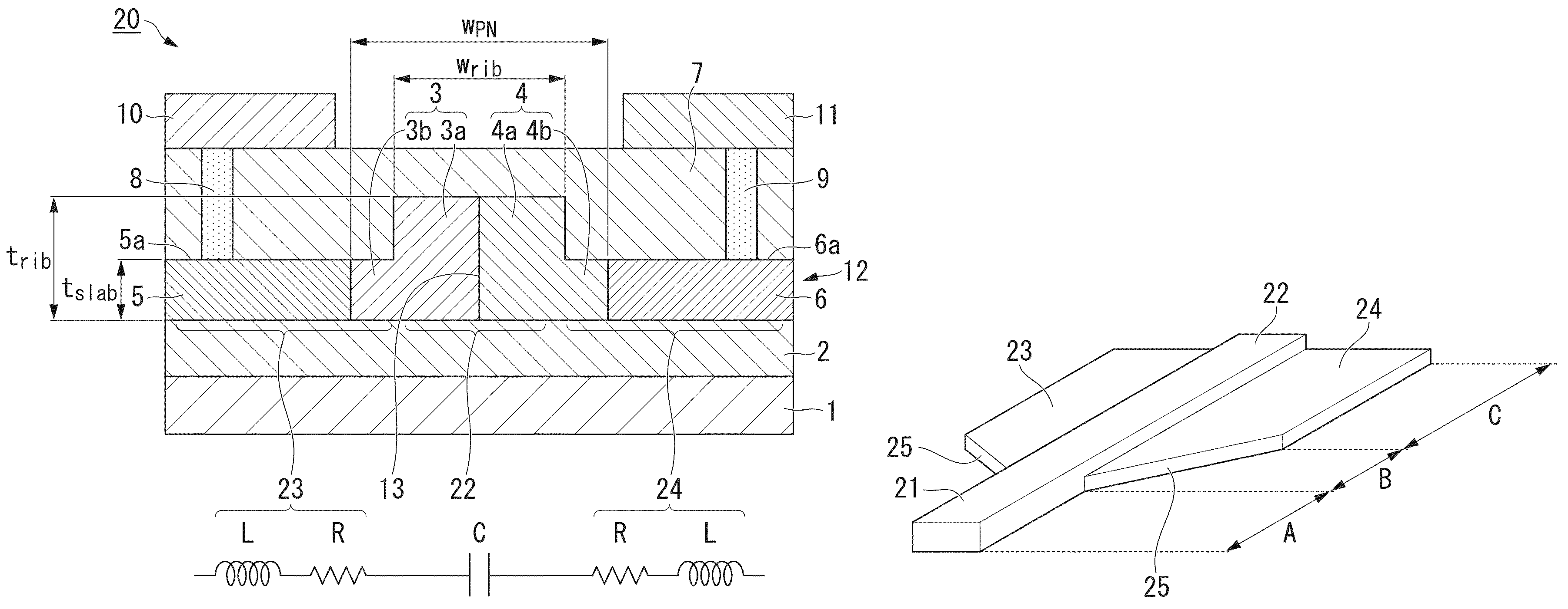
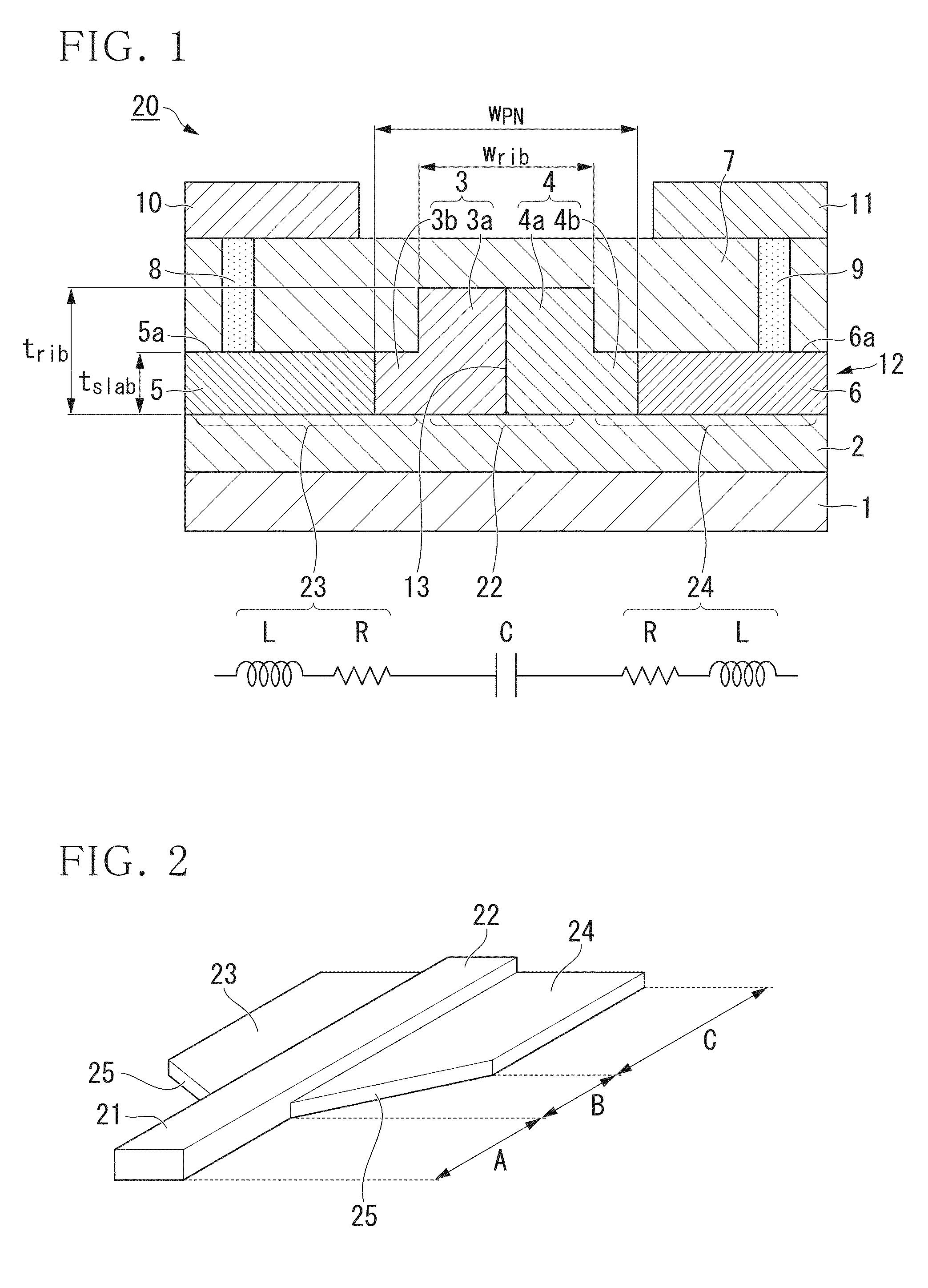
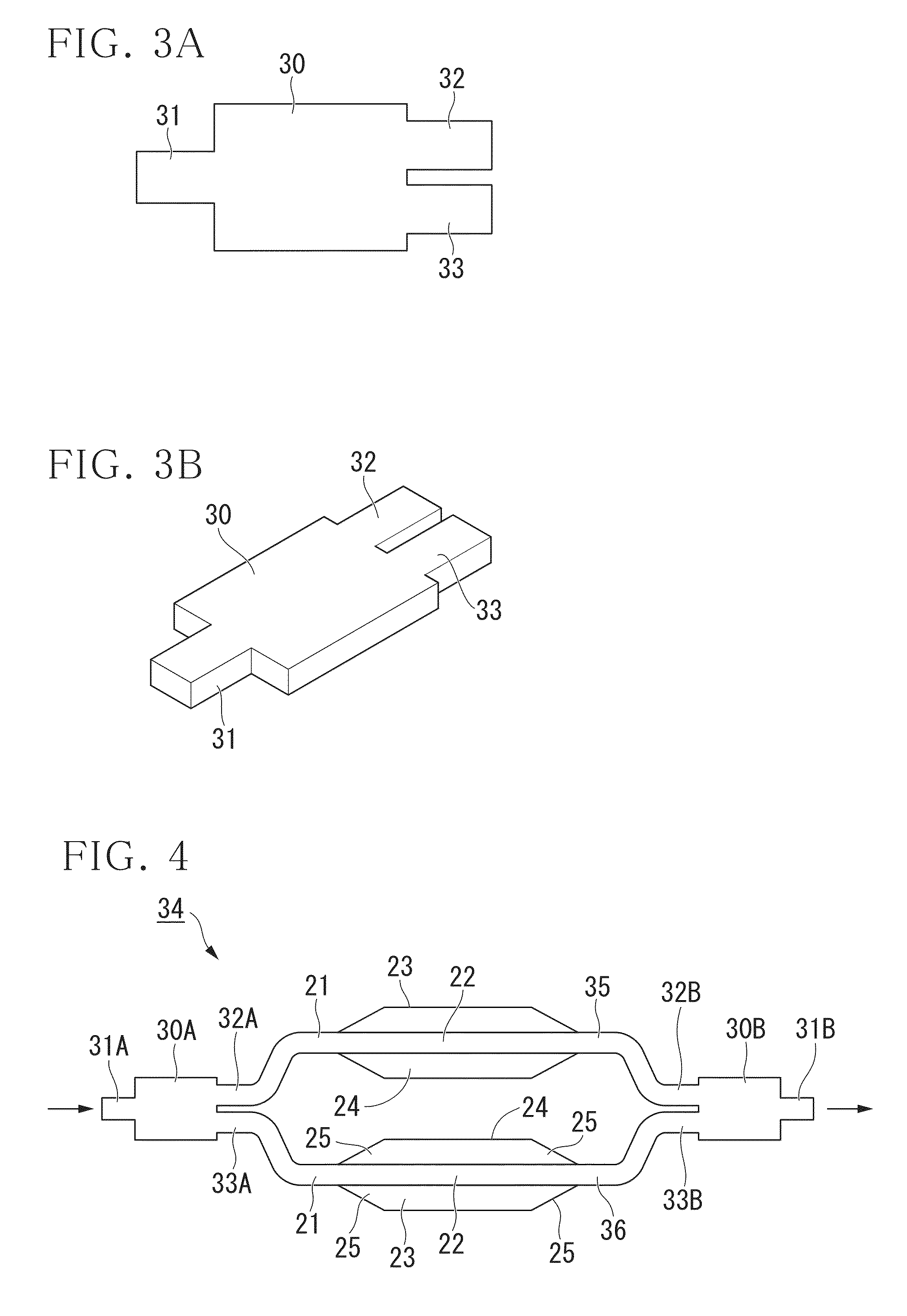
[0106]In the configuration shown in FIG. 1, an SOI wafer was used as the material for the substrate 1, the lower cladding 2, and the core 12. A BOX layer made of silica having a thickness of 2 μm was formed as the lower cladding 2, and a P-type or N-type dopant was added to an overlying SOI layer made of silicon by ion implantation to form the P-type semiconductor 3, the N-type semiconductor 4, the P-type conductor 5, and the N-type conductor 6. A part of the core 12 was removed by etching to form the rib portion 22 and the slab portions 23 and 24. The rib width wrib was 500 to 600 nm, the rib thickness trib was 220 nm, the slab thickness tslab was 95 nm, and the interval wPN of the P-type conductor 5 and the N-type conductor 6 was about 2 μm. The upper cladding 7 made of silica was deposited at a thickness of about 1 to 2 μm by CVD or the like. Through holes formed in the upper cladding 7 were...


PUM


Abstract

An optical waveguide element includes: a rib waveguide and a pair of slab portions including a first slab portion and a second slab portion connected to both sides of the rib portion so as to sandwich the rib portion. The rib portion has a cross-sectional dimension which allows the propagation of a fundamental mode and a higher order mode in a predetermined single polarization state, and has a first P-type semiconductor and a first N-type semiconductor forming a PN junction, the first slab portion has a second P-type semiconductor and a P-type conductor connected to each other, the second P-type semiconductor is connected to the first P-type semiconductor of the rib portion, the second slab portion has a second N-type semiconductor and an N-type conductor connected to each other, and the second N-type semiconductor is connected to the first N-type semiconductor of the rib portion.

Description

CROSS REFERENCE TO RELATED APPLICATIONS[0001]This application is a continuation application based on a PCT Patent Application No. PCT / JP2013 / 073828, filed Sep. 4, 2013, whose priority is claimed on Japanese Patent Application No. 2012-283964 filed Dec. 27, 2012, the entire contents of which are hereby incorporated by reference.BACKGROUND OF THE INVENTION[0002]1. Field of the Invention[0003]The present invention relates to an optical waveguide element having high speed and low optical loss, and an optical modulator including the optical waveguide element.[0004]2. Description of the Related Art[0005]In recent years, the use of an optical integrated circuit, such as a planar optical waveguide, in a device for optical fiber communication, especially, long-distance wavelength multiplex optical fiber communication, has been considered.[0006]PCT International Publication No. WO95 / 08787 discloses a single-mode silicon rib waveguide which has a PIN junction in a lateral direction and changes...

Claims


Application Information

Patent Timeline
IPC IPC(8): G02F1/025G02B6/122G02B6/12G02F1/015G02F1/21
CPCG02F1/025G02B6/1228G02F1/015G02B2006/12061G02B2006/12097G02B2006/12159G02F2001/0152G02F2001/212G02F1/2257G02F1/0152G02F1/212
Inventor OGAWA, KENSUKEGOI, KAZUHIROKUSAKA, HIROYUKI
Owner THE FUJIKURA CABLE WORKS LTD
Learn More