Transistor device structure that includes polycrystalline semiconductor thin film that has large grain size
a polycrystalline semiconductor and thin film technology, applied in the direction of semiconductor devices, semiconductor devices, electrical equipment, etc., can solve the problems of high manufacturing cost, short channel effect (sce) and high leakage current, and manufacturing processes developed from the above technologies have faced specific difficulties and bottlenecks, and achieve the effect of simple manufacturing process features and low manufacturing cos
- Summary
- Abstract
- Description
- Claims
- Application Information
AI Technical Summary
Benefits of technology
Problems solved by technology
Method used
Image

Examples
Embodiment Construction
[0019]The present invention will now be described more specifically with reference to the following embodiments. It is to be noted that the following descriptions of preferred embodiments of this invention are presented herein for purpose of illustration and description only. It is not intended to be exhaustive or to be limited to the precise form disclosed.
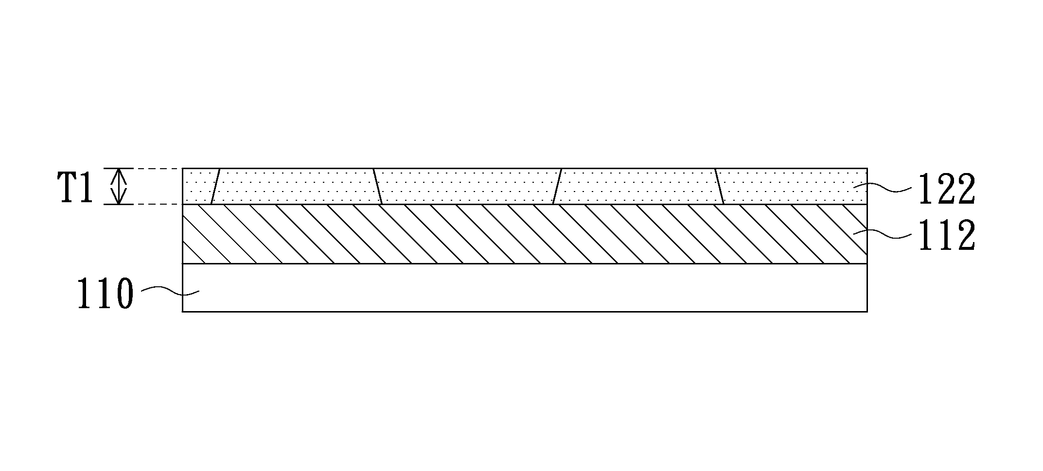
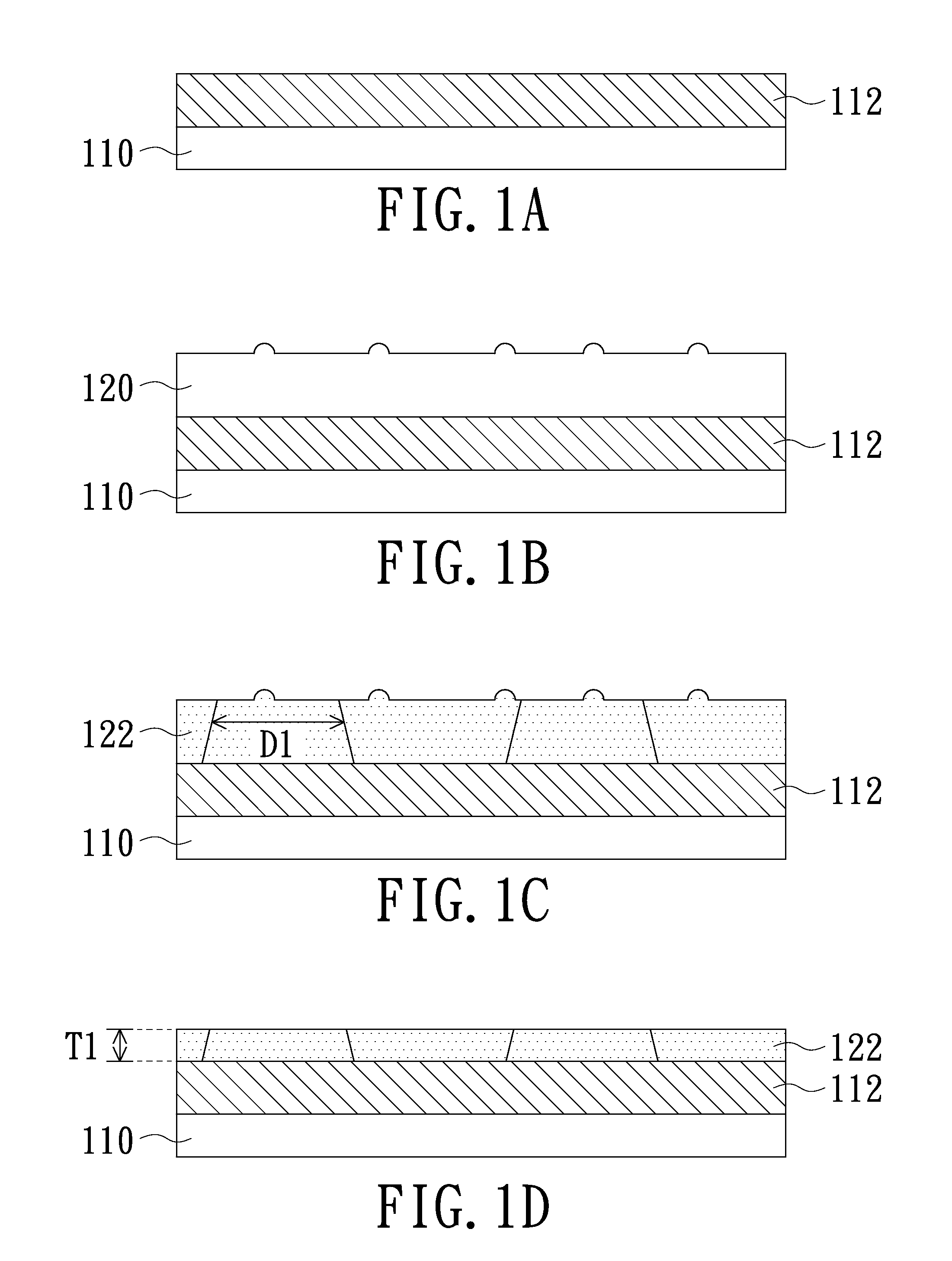
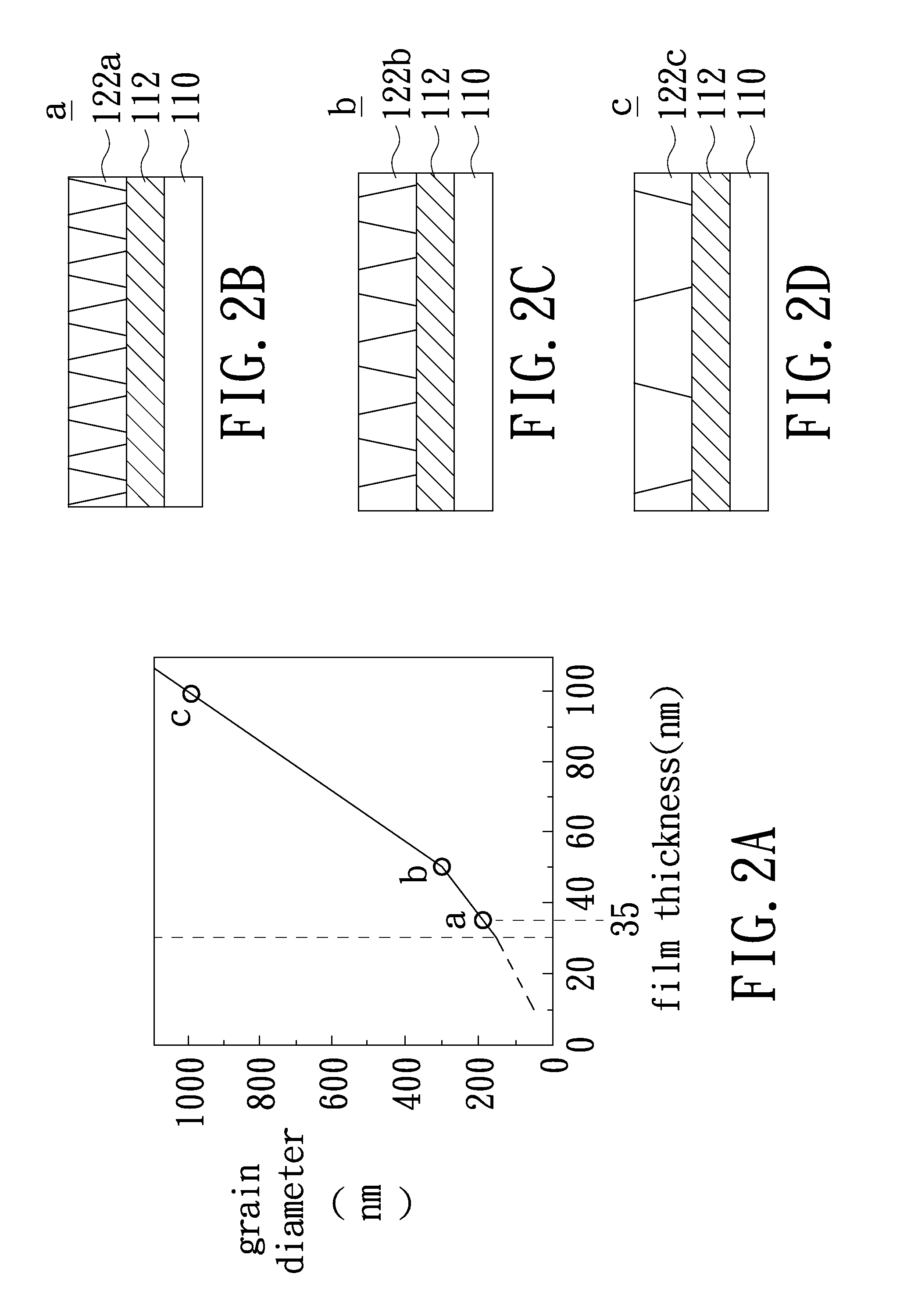
[0020]FIGS. 1A˜1D are schematic diagrams illustrating a process of a method for manufacturing a polycrystalline semiconductor thin film in accordance with an embodiment of the present invention. Please refer to FIGS. 1A˜1C first. As shown, the method in this embodiment includes the following steps. First, a substrate is provided. The substrate may include a semiconductor substrate 110 and a first insulating material layer 112. Specifically, the first insulating material layer 112 is formed on a surface of the semiconductor substrate 110, as illustrated in FIG. 1A. The semiconductor substrate 110 may be a silicon (Si) substrate; a...
PUM
| Property | Measurement | Unit |
|---|---|---|
| thickness | aaaaa | aaaaa |
| grain diameter | aaaaa | aaaaa |
| thickness | aaaaa | aaaaa |
Abstract
Description
Claims
Application Information