Article and method for implementing electronic devices on a substrate using quantum dot layers

a technology of quantum dots and electronic devices, applied in the direction of optical elements, optical waveguide light guides, instruments, etc., can solve the problems of difficult to tune waveguides and other components

Active Publication Date: 2016-11-15
JAIN FAQUIR CHAND +1
View PDF16 Cites 16 Cited by
  • Summary
  • Abstract
  • Description
  • Claims
  • Application Information

AI Technical Summary

Benefits of technology

[0005]A photonic waveguide having three layers is provided and includes a top layer having a top layer index of refraction (TIOR); a bottom layer having a bottom layer index of refraction (BIOR); and a middle layer, wherein the middle layer includes a middle layer effective index of refraction (MIOR) that is greater than the TIOR and the BIOR and regions adjacent to it vertically as well as laterally, wherein the top layer, bottom layer and middle layer are deposited on a substrate which is selected from at least one of Si, Ge, Si-on-Insulator, Si-on-sapphire, GaAs, InP, ZnSe, LiNbO3 and any material with similar characteristics of at least one of Si, Ge, Si-on-Insulator, Si-on-sapphire, GaAs, InP, ZnSe, LiNbO3, wherein the middle layer serves as the waveguiding layer where photons are confined in the transverse and lateral directions by regions characterized by at least one of a lower index of refraction and photonic crystal structure which includes two-dimensional or three-dimensional lattice photonic crystals, and wherein the middle layer is constructed of an array of cladded quantum dots, wherein the cladded quantum dots have a core with a diameter in the range of about 3 nm to about 5 nm and a cladding of higher energy gap and lower index of refraction material in the range of about 1 nm to about 3 nm, wherein the middle waveguide layer optical parameters include an effective index of refraction, coefficient of absorption at a given light wavelength, wherein their magnitude is at least partially dependent on at least one of a relative core diameter, cladding thickness and the materials of quantum dots comprising the middle layer, wherein the middle layer optical parameters can be altered by applying an external voltage and associated electric field, and wherein the core is selected from at least one of Si, Ge, Si, combination of Si and Ge, II-VI and III-V semiconductors, and any combination thereof, and wherein the cladding on the quantum dot is selected from at least one of SiOx, GeOx, II-VI and III-V materials, and any combination thereof, and wherein the top layer deposited above the middle layer is constructed from a material selected from at least one of SiO2, Si3N4, SiON, and any suitable lower index of refraction and higher energy gap materials, and wherein the bottom layer below the middle layer is constructed from a material selected from at least one of SiO2, Si3N4, SiON, and any suitable lower index of refraction and higher energy gap materials, and wherein the cladding layers incorporating an electrode material layer for the purpose of applying an external voltage bias and / or signal for modulation, the top cladding layer is deposited with an electrode layer to apply external voltages, the substrate or bottom cladding layer incorporating a deposited electrode through which to apply the the external electric field, the waveguiding structure comprising of middle waveguide layer, top and bottom cladding layer realized in conjunction with either lower index refraction cladding regions or photonic crystal structure along the two lateral sides adjoining the waveguiding structure.
[0006]A nanophotonic waveguide is provided and includes three layers, a middle layer having an effective index of refraction higher than the upper and bottom cladding layers and regions adjacent to it vertically as well as laterally, the three layers are deposited on a substrate which is selected from Si, Ge, Si-on-Insulator, Si-on-sapphire, GaAs, InP, ZnSe, and LiNbO3, the middle layer serving as the waveguiding layer where photons are confined in the transverse and lateral directions by lower index of refraction regions or photonic crystal structure comprising of 2-dimensional or 3-dimensional lattice photonic band gap structures, the middle waveguding layer is made of semiconductor selected from Si, Ge, SixGe1-x, III-VI and II-VI semiconductors, the three layers forming the waveguide are surrounded in the lateral direction by a layer or regions comprised of cladded quantum dot layer, the quantum dot array having a core with diameter in the range of 3-5 nm and a cladding of higher energy gap and lower index of refraction material in the range of 1-3 nm, the quantum dot layer (adjoining the middle, upper and lower waveguide structure) having its optical parameters including effective index of refraction, coefficient of absorption at given light wavelength depend on relative core diameter, cladding thickness and the materials of quantum dots comprising the middle layer, the adjoining layer optical parameters can be altered by applying an external voltage and its associated electric field, the core of the quantum dot layer is selected from Si, Ge, Si, combination of Si and Ge, II-VI and III-V semiconductors, the cladding on quantum dot is selected from SiOx, GeOx, II-VI and III-V materials, the quantum dot layers having on top an electrode material layer for the purpose of applying an external voltage bias and / or signal for modulation, the quantum dot layers having on bottom side an electrode material layer for the purpose of applying an external voltage bias and / or signal for modulation, the electrode material layer on bottom side of quantum dot layer could be deposited on the bottom side of substrate to apply the said external electric field.
[0007]A nano-photonic waveguide is provided and includes three layers, a middle layer having an effective index of refraction higher than those of the top and bottom cladding layers and regions adjacent to it vertically as well as laterally, the three layers are deposited on a substrate which is selected from Si, Ge, Si-on-Insulator, Si-on-sapphire, GaAs, InP, ZnSe, and LiNbO3 the middle layer serving as the waveguiding layer where photons are confined in the transverse and lateral directions by regions characterized by lower index of refraction or photonic crystal structure comprising of two-dimensional or three-dimensional lattice photonic crystals, the middle waveguding layer is composed of an array of cladded quantum dots, the quantum dot array having a core with diameter in the range of 3-5 nm and a cladding of higher energy gap and lower index of refraction material in the range of 1-3 nm, the middle waveguide layer optical parameters including effective index of refraction, coefficient of absorption at given light wavelength, wherein their magnitude is dependent on relative core diameter, cladding thickness and the materials of quantum dots comprising the middle layer, the middle layer optical parameters can be altered by applying an external voltage and associated electric field, the core is selected from Si, Ge, Si, combination of Si and Ge, II-VI and III-V semiconductors, the cladding on quantum dot is selected from SiOx, GeOx, II-VI and III-V materials, a top cladding layers deposited above the middle waveguide layer is selected from SiO2, Si3N4, SiON, and lower index of refraction and higher energy gap materials, a bottom cladding layer below the middle layer having its material selected from SiO2, Si3N4, SiON, and lower index of refraction and higher energy gap materials, the cladding layers incorporating an electrode material layer for the purpose of applying an external voltage bias and / or signal for modulation, the top cladding layer is deposited with an electrode layer to apply external voltages, the substrate or bottom cladding layer incorporating a deposited electrode through which to apply the the external electric field, the waveguiding structure comprising of middle waveguide layer, top and bottom cladding layer realized in conjunction with either lower index refraction cladding regions or photonic crystal structure along the two lateral sides adjoining the waveguiding structure.

Problems solved by technology

However, once fabricated it is generally difficult to tune the waveguides and other components.

Method used


Image

  • Article and method for implementing electronic devices on a substrate using quantum dot layers
  • Article and method for implementing electronic devices on a substrate using quantum dot layers
  • Article and method for implementing electronic devices on a substrate using quantum dot layers

Examples


Embodiment Construction

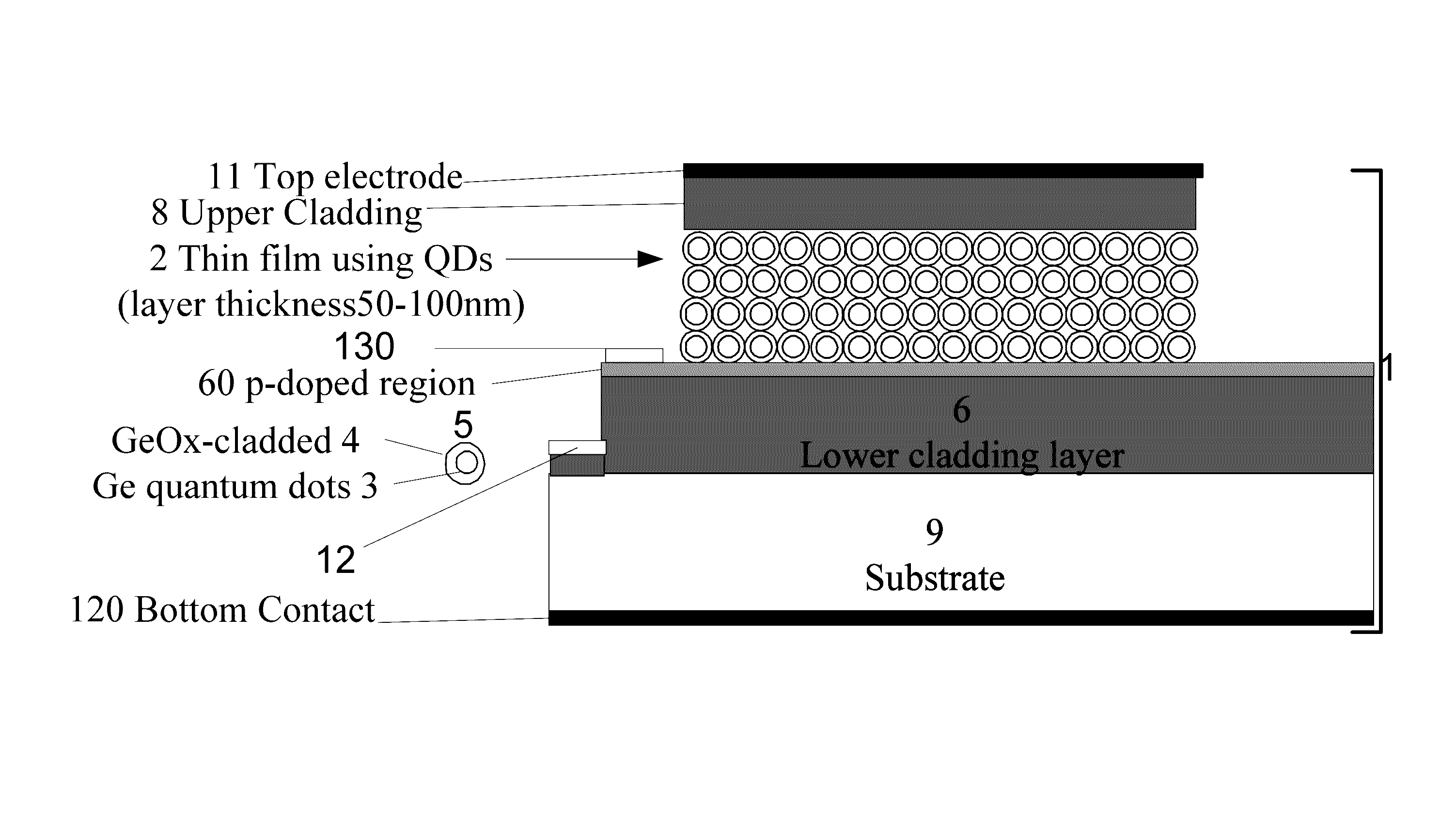
[0050]The limitations of the prior art identified above are overcome by employing cladded quantum dot based waveguides and cladding layers which can be tuned after fabrication. This feature also permits reconfiguration of demultiplexers, routers, channel drop filters and other devices needed in the realization of ultra-compact photonic integrated circuits.

[0051]In accordance with the present invention, an article and method is described where the method uses a cladded quantum dot array layer as a waveguide channel sandwiched between two cladding layers which includes index of refraction materials lower than the waveguide layer. This is advantageous because, unlike conventional waveguide layers, the overall effective index of refraction in a quantum dot array layer depends on: (1) dot and cladding material properties, and (2) the core diameter and cladding thickness. The cladded quantum dot layer hosts excitons in the presence of an optical wave signal having an appropriate wavelengt...


PUM

PropertyMeasurementUnit
thicknessaaaaaaaaaa
diameteraaaaaaaaaa
diameteraaaaaaaaaa

Abstract

Novel use of a cladded quantum dot array layer serving as a waveguide channel by sandwiching it between two cladding layers comprised of lower index of refraction materials is described to form Si nanophotonic devices and integrated circuits. The photonic device structure is compatible with Si nanoelectronics using conventional, quantum dot gate (QDG), and quantum dot channel (QDC) FET based logic, memories, and other integrated circuits.

Description

CROSS REFERENCE TO RELATED APPLICATIONS[0001]This application claims benefit of the filing data of U.S. Provisional Patent Application Ser. No. 61 / 676,639, filed Jul. 27, 2012, the contents of which are incorporated by reference herein in its entirety.STATEMENT REGARDING FEDERALLY SPONSORED RESEARCH[0002]The United States Government has certain rights in this invention pursuant to Office of Naval Research (ONR) Grant No. N00014-06-1-0016.FIELD OF THE INVENTION[0003]The present invention relates generally to the implementation of electronic devices on a substrate and more particularly to the use of Quantum Dot Layers to implement electronic devices on a substrate, including Si nanophotonics, photonic crystal and photonic band gap waveguides, quantum dot waveguides and claddings, Mach-Zehnder interferometer and directional coupler optical modulators, and multiplexers and demultiplexers.BACKGROUND OF THE INVENTION[0004]Silicon nanophotonic waveguides implemented in conventional and pho...

Claims


Application Information

Patent Timeline
Patent Type & Authority Patents(United States)
IPC IPC(8): G02B6/10G02F1/017G02F1/035B82Y20/00
CPCG02F1/01708G02F1/035G02B6/10G02F2001/01791Y10S977/774Y10S977/932B82Y20/00G02B6/122G02B6/1225G02F1/2255G02F1/2257G02F2202/32G02F1/212G02F1/01791G02B6/12004G02B2006/12121G02B2006/12142G02F2202/103G02F2202/107
Inventor JAIN, FAQUIR CHANDZELLER, JOHN
Owner JAIN FAQUIR CHAND
Why Eureka
Try Eureka