

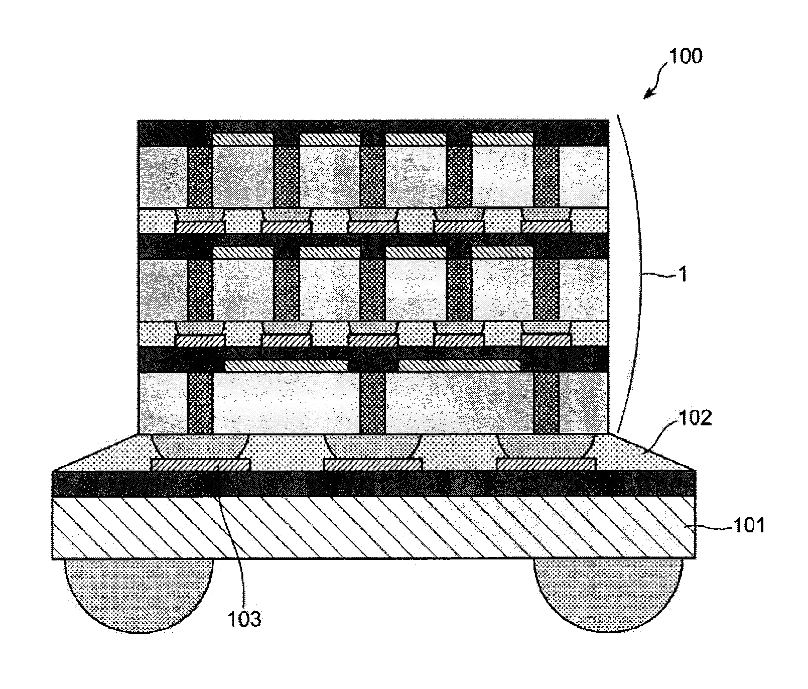
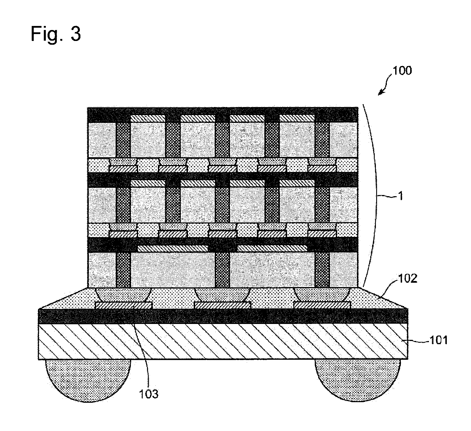
Three-dimensional integrated circuit laminate, and interlayer filler for three-dimensional integrated circuit laminate
a technology of interlayer filler and integrated circuit, which is applied in the direction of transportation and packaging, basic electric elements, solid-state devices, etc., can solve the problems of low thermal conductivity of interlayer filler composition, loss of performance, etc., and achieve low linear thermal expansion property, excellent reliability, and high thermal conductivity
- Summary
- Abstract
- Description
- Claims
- Application Information
AI Technical Summary
Benefits of technology
Problems solved by technology
Method used
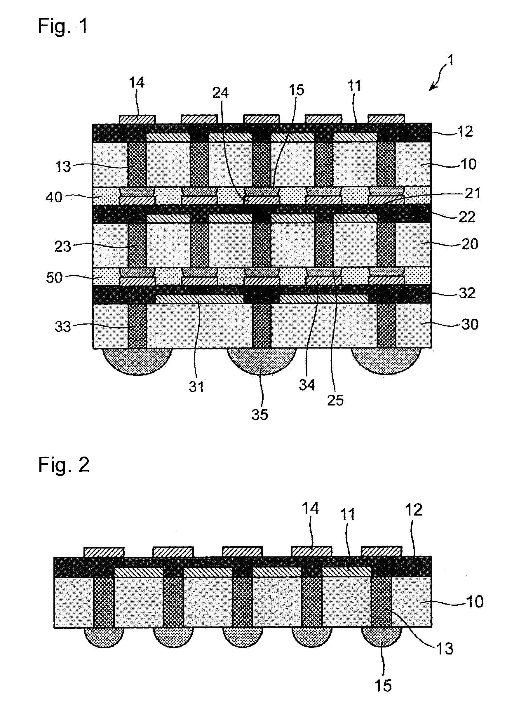
Image

Examples
example 1
[0247]45 parts by weight of epoxy resin (A2-1), 5 parts by weight of reactive diluting agent (A4) and 50 parts by weight of inorganic filler (B-1) were mixed, and the mixture was passed through a three-roll mill of which the roll distance was adjusted to 10 μm five times to obtain a mixture paste of the epoxy resin / the inorganic filler.
[0248]The average particle size of the inorganic filler (B-1) in the mixture paste of the epoxy resin / the inorganic filler was 0.6 μm. Further, the specific surface area of the inorganic filler (B-1) was 9.69 m2 / g.
[0249]5 parts by weight of curing agent (C-1) was added to 100 parts by weight of the mixture paste of the epoxy resin / the inorganic filler, followed by mixing by a rotary and revolutionary mixing apparatus (“Awatori Rentaro”, tradename, manufactured by THINKY CORPORATION) at 2,000 revolutions under conditions of mixing for 5 minutes and bubble removal for one minute.
[0250]The mixed paste was sandwiched between glass plates subjected to rele...
example 2
[0251]The same operation as in Example 1 was carried out except that inorganic filler (B-2) was used instead of inorganic filler (B-1) in Example 1.
[0252]The average particle size of the inorganic filler (B-2) by the above measurement method was 4.1 μm. Further, the specific surface area of the inorganic filler (B-2) was 16 m2 / g.
[0253]Of the obtained interlayer filler composition film, the thermal conductivity was 0.5 W / (m·K) and the dielectric constant was 3.2. Further, the dielectric constant was calculated from the volume fraction of the filler component in the interlayer filler composition based on the dielectric constants (epoxy resin: 2.8, boron nitride: 3.9) of the respective materials.
example 3
[0254]As epoxy resin (A), 5 g of the epoxy resin (A1) solution, 3.75 g of epoxy resin (A2-2), 0.94 g (80 wt % cyclohexanone solution) of epoxy resin (A2-3), 2.14 g (70 wt % cyclohexanone solution) of epoxy resin (A2-4), 7.24 g of inorganic filler (B-1) and further, 24.0 g of zirconia balls (YTZ-2) having a diameter of 2 mm were added, followed by stirring by a rotary and revolutionary stirring machine at 2,000 rpm for 33 minutes. After completion of stirring, the beads were removed by filtration, and 0.15 g of curing agent (C-2) and 0.15 g of flux (D-1) were added, followed by further stirring by a rotary and revolutionary stirring machine for 6 minutes to obtain an interlayer filler paste (coating fluid).
[0255]The particle size distribution of inorganic filler (B-1) in the obtained interlayer filler paste after stirring was measured, whereupon the average particle size was 1.0 μm and the maximum particle size was 5.9 μm.
[0256]This material paste was applied to a glass substrate sub...
PUM
 Abstract
Description
Claims
Application Information