Resistive random access memory with high uniformity and low power consumption and method for fabricating the same

a random access and high uniformity technology, applied in the field of resistive random access memory, can solve the problems of affecting the achievement of low power consumption, advancing resistive random access, and increasing the severity of reliability problems, and achieve the effects of low power consumption storage, high uniformity, and controlled accurately

Inactive Publication Date: 2016-12-20
PEKING UNIV
View PDF26 Cites 0 Cited by
  • Summary
  • Abstract
  • Description
  • Claims
  • Application Information

AI Technical Summary

Benefits of technology

[0005]Based on the concerns as above, the present invention may achieve complete formation-rupture of oxygen vacancy conductive filaments (CF) in each layer by dividing a resistive material film of the same metal oxide into four layers according to the different oxygen concentrations, so as to control accurately the resistance values, so that 2-bit storage with high uniformity is achieved. In addition, by adjusting properly the resistance value of each layer of the four-layer structure, low current operation can be performed, and thus the low power consumption can be achieved. At the same time, according to the principle of the present invention, the storage of 3-bit and more density can be further achieved.
[0020]The resistive random access memory design proposed by the present invention mainly has the following three advantages:
[0021](1) the fabricating processing is compatible with CMOS processing, and compared with a general RRAM, no new process step is added, the operation being simple and easy to implement.
[0023]As described above, by making the complete formation-rupture occur in the conductive filament in a corresponding one of layers each time, the corresponding four states may be controlled accurately, thereby 2-bit storage with high uniformity may be achieved.
[0024](3) furthermore, because the resistance value of each layer may be adjusted by the processing, when the resistance value of each layer is set to be larger, the current of the corresponding resistance state of the device is smaller, thereby the low power consumption storage may be achieved.

Problems solved by technology

In recent years, as the device size continue to shrink, especially after progressing to the nano-sized nodes, the shrinking ability (scaling) of NVM devices such as Flash in a current mainstream will reach a limit, random fluctuation is increased significantly, the reliability problems become increasingly severe. in view of this, researchers have proposed in succession some new memories such as the electric charge trap memory (CTM), ferroelectric random access memory (FeRAM), a magnetic random access memory (MRAM), phase change random access memory (PRAM), resistive random access memory and so on.
Nevertheless, further development of resistive random access memory is still facing many challenges, which is embodied significantly in some aspects such as the uniformity concern of the operating voltage and resistance state, the reliability concern such as endurance and retention, large reset current which hinders the achievement of low power consumption, how to achieve higher density integration and so on.
However, the formation-rupture of CF in general resistive random access memory occurs in a single resistive layer, due to the greater random fluctuation of the width of CF (or the oxygen vacancy concentration in CF) and the gap adjusting, the uniformity concern is serious, that is, the overlapping occurs between different resistance states.

Method used


Image

  • Resistive random access memory with high uniformity and low power consumption and method for fabricating the same
  • Resistive random access memory with high uniformity and low power consumption and method for fabricating the same
  • Resistive random access memory with high uniformity and low power consumption and method for fabricating the same

Examples


embodiment 1

[0043

[0044]The present invention is described below in further detail with TaOx resistive random access memory as an example with reference to the accompanying drawings and specific embodiments.

[0045]The fabrication process for 2-bit resistive random access memory cell with high uniformity and low power consumption in accordance with the present invention is provided as follows:

[0046]1) preparing an insulating layer, comprising growing SiO2 on a Si substrate 1 as the insulating layer 2, as shown in FIG. 7;

[0047]2) preparing a bottom electrode, comprising sputtering metal Ti / M, wherein Ti is used for an adhesion layer, M is used for the bottom electrode 3, as shown in FIG. 8, M is a conductive metal or a metal nitride, such as Pt, Ag, Ir, Ru, Au, Pd, W, Ni, Cu, Ti, TiN, TaN, WNx or the like;

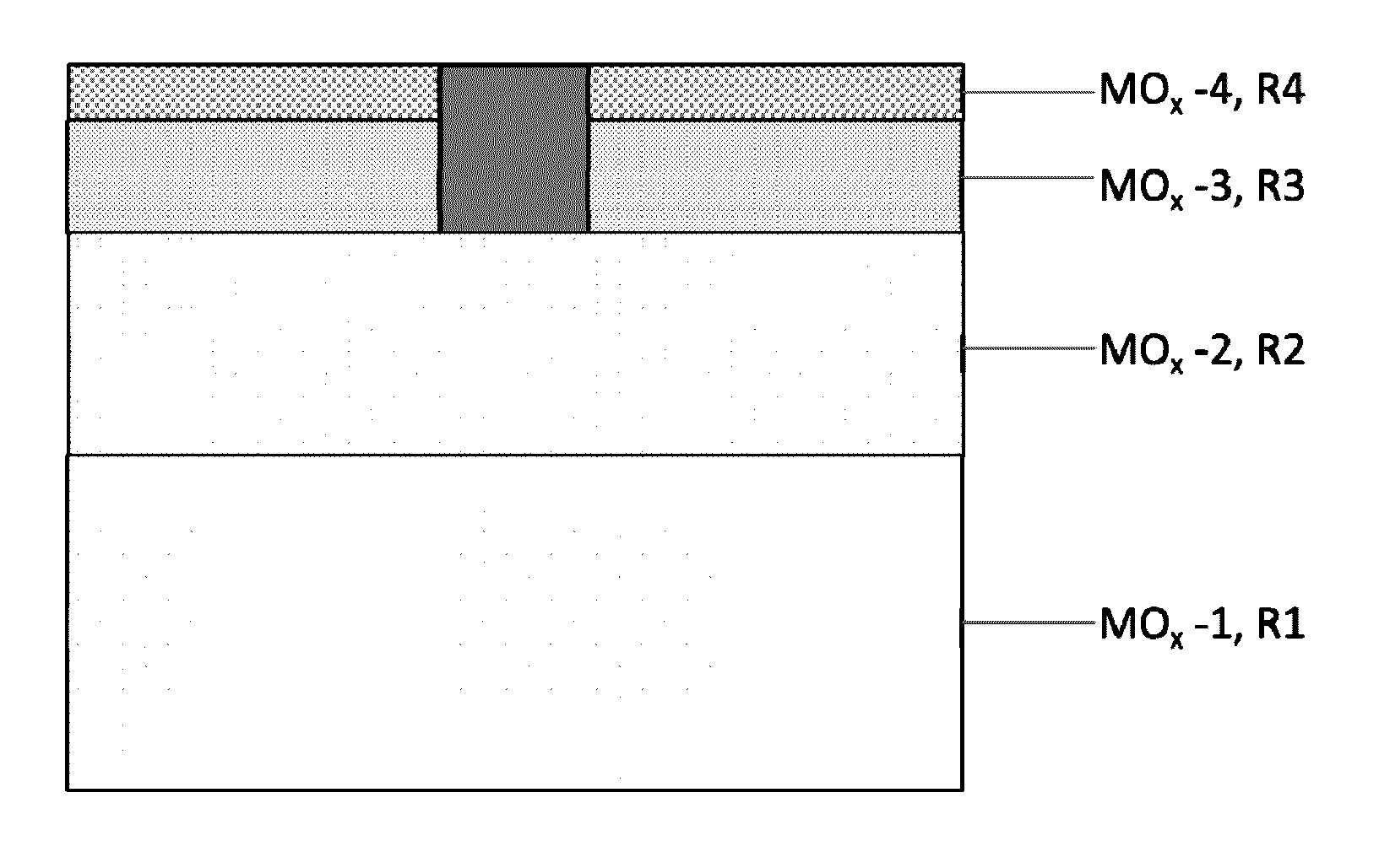
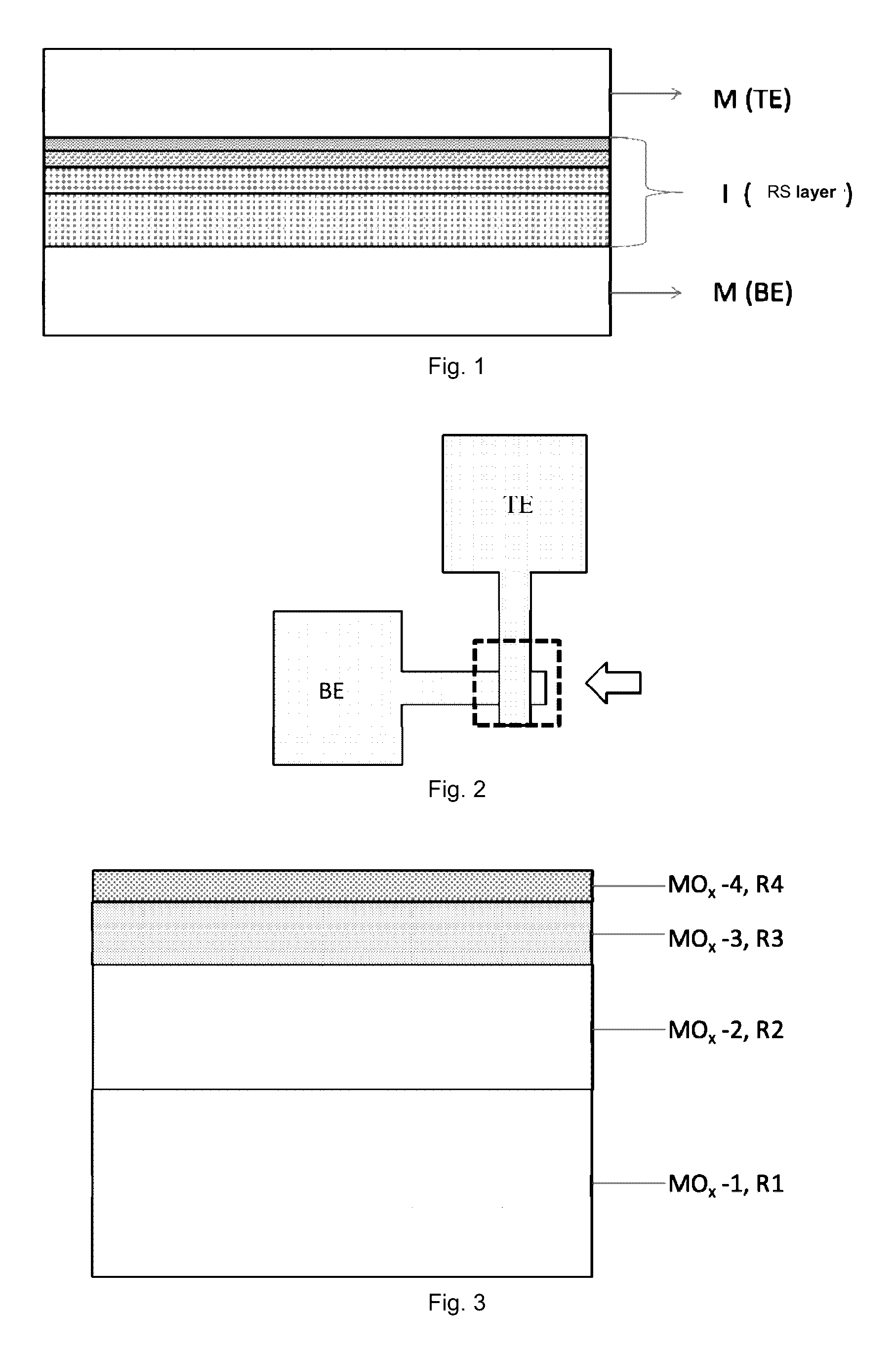
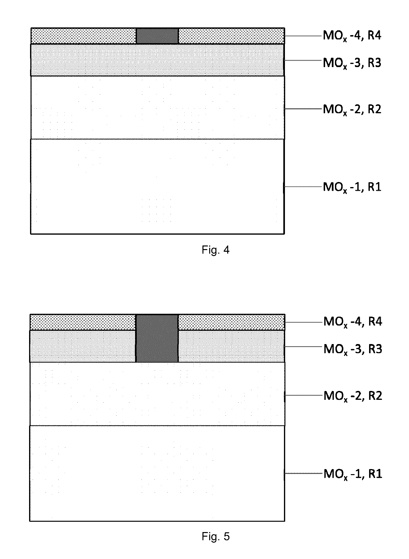
[0048]3) preparing a first layer of resistive material film, wherein the first layer 4-1 of TaOx resistive material film is prepared, with a thickness of 30 nm, oxygen partial pressure of 3% and a...


PUM


Abstract

Disclosed is a resistive random access memory, comprising a substrate, an insulating layer, a bottom electrode, a resistive material film, and a top electrode in an order from bottom to top, wherein the resistive material film is a four-layer structure composed of a same metal oxide; and the four layers in the four-layer structure from bottom to top have resistance values which are increased one after another by more than 10 times, oxygen concentrations which are increased one after another and thickness which are decreased one after another. The present invention may achieve complete formation-rupture of oxygen vacancy conductive filaments (CF) in each layer by dividing the resistive material film of the same metal oxide into four layers according to the different oxygen concentrations, so as to control accurately the resistance values, so that 2-bit storage with high uniformity is achieved.

Description

CROSS REFERENCE TO RELATED APPLICATION[0001]This application is entering into the national phase of PCT application No. PCT / CN2014 / 074369, filed on Mar. 31, 2015, which claims priority of Chinese Patent Application (No. 201310618361.8), filed on Nov. 28, 2013, which is incorporated herein by reference in its entirety.TECHNICAL FIELD[0002]The invention relates to a resistive random access memory (RRAM), and particularly relates to a design for a 2-bit resistive random access memory cell with high uniformity and low power consumption and a method for fabricating the same, which belongs to a field of nonvolatile memory performance optimization in CMOS ultra large scale integrated circuit (ULSI) and the fabrication technology thereof.BACKGROUND OF THE INVENTION[0003]In recent years, as the device size continue to shrink, especially after progressing to the nano-sized nodes, the shrinking ability (scaling) of NVM devices such as Flash in a current mainstream will reach a limit, random fl...

Claims


Application Information

Patent Timeline
Patent Type & Authority Patents(United States)
IPC IPC(8): H01L29/00H01L47/00H01L21/336H01L45/00
CPCH01L45/146H01L45/08H01L45/1233H01L45/1616H01L45/1625H01L45/1675H10N70/24H10N70/826H10N70/8833H10N70/026H10N70/023H10N70/063
Inventor HUANG, RUYU, MUXICAI, YIMAOZHANG, ZHENXINGLI, QIANGLI, MING
Owner PEKING UNIV
Why Eureka
Try Eureka