Method and device for generating short optical pulses

a technology of optical pulses and optical pulses, which is applied in the direction of semiconductor lasers, laser details, active medium shape and construction, etc., can solve the problems of limiting the maximum achievable peak power of the laser, low average power in the order typical limited average power of a few mw, so as to achieve high power output, reduce power density per facet area, and reduce leakage losses

Active Publication Date: 2017-01-10
TECH UNIV BERLIN
View PDF6 Cites 0 Cited by
  • Summary
  • Abstract
  • Description
  • Claims
  • Application Information

AI Technical Summary

Benefits of technology

[0043]The multi-layered sequence has preferably non-uniform doping by n-type impurity with increased concentration in the layers of localization of the higher order modes contiguous to the substrate with larger leakage and total internal losses of the higher order modes as compared to that of the fundamental mode.
[0051]The multi-layered sequence preferably has non-uniform doping by p-type impurity with increased concentration in the layers of localization of the higher order modes contiguous to the contact layer with larger leakage and total internal losses of the higher order modes as compared to that of the fundamental mode.
[0061]This lasers presented above provide high power and simultaneously small divergence of the output radiation in the vertical direction (direction of the epitaxial growth). The lasers are based on the realization that a laser waveguide consisting of a layer with an active region and multiple epitaxial layers, which are stacked on top of a high refractive index substrate in the direction perpendicular to the light propagation forming specific aperiodic sequences with a proper choice of the thicknesses and refractive indices of all the layers as functions of the vertical distance, providing expansion of the fundamental mode and attenuation of the higher order modes. The expanded fundamental mode is localized predominantly at the layer containing the active region and all higher order modes predominantly at the multiple layers. The multiple epitaxial layers are adjusted to provide also higher leakage losses into the substrate and / or contact layer of all higher order modes as compared to that of the fundamental mode. Localization of the modes and their leakage are controlled by the relations between the effective indices of the modes and the refractive indices of the active layer and the substrate (and / or contact layer), respectively. Because of selection by the confinement factor and the leakage losses in favor of the fundamental mode, the output radiation is single-mode and results in a single-lobe far field with small divergence in the vertical direction. Since the power density per facet area is decreased upon broadening the waveguide and expanding the fundamental mode, high power output is also made possible before the onset of thermal and current spreading, catastrophic optical mirror damage and other nonlinear optical effects. The lasers are applicable to essentially any semiconductor laser diode system based on (Al,Ga,In)(As,P,Sb,N) or other semiconductor heterostructures emitting in the infra-red, red, visible or UV wavelength ranges.

Problems solved by technology

Besides, the average power is typically limited to a few mW due to the low duty cycle of the electrical pulse train used to forward bias the laser diode.
However, in order to obtain short picosecond pulses, the two-section laser needs to be driven with high reverse absorber bias in the absorber section and low injection currents in the gain section, also resulting in very low average powers in the order of a few mW.
Another factor severely limiting the maximum achievable peak power of the laser is catastrophic optical damage as a consequence of the increase in optical power density when short optical pulses propagate within the cavity.
Furthermore, as high peak power pulses are absorbed by the saturable absorber section, a high photocurrent is generated causing catastrophic damage of the absorber element.
Additionally, fabrication of the laser diode requires extra processing steps as well as more challenging post-processing techniques, particularly if the laser is to be p-side down bonded for efficient heat dissipation.
In both techniques, the low average power level is not sufficient for the aforementioned applications, which are currently being addressed by costly Ti:sapphire or fiber lasers providing average powers in the Watt level or more.
Besides being a complex solution which is less compact and cost effective, another disadvantage of this configuration arises when amplifying ultra-short optical pulses in the ps or fs range due to the very high peak power levels generated within the amplifier, leading to detrimental nonlinear pulse distortion and damage of the gain medium.

Method used


Image

  • Method and device for generating short optical pulses
  • Method and device for generating short optical pulses
  • Method and device for generating short optical pulses

Examples


Embodiment Construction

[0081]The preferred embodiments of the present invention will be best understood by reference to the drawings, wherein identical or comparable parts are designated by the same reference signs throughout.

[0082]It will be readily understood that the present invention, as generally described herein, could vary in a wide range. Thus, the following more detailed description of the exemplary embodiments of the present invention, is not intended to limit the scope of the invention, as claimed, but is merely representative of presently preferred embodiments of the invention.

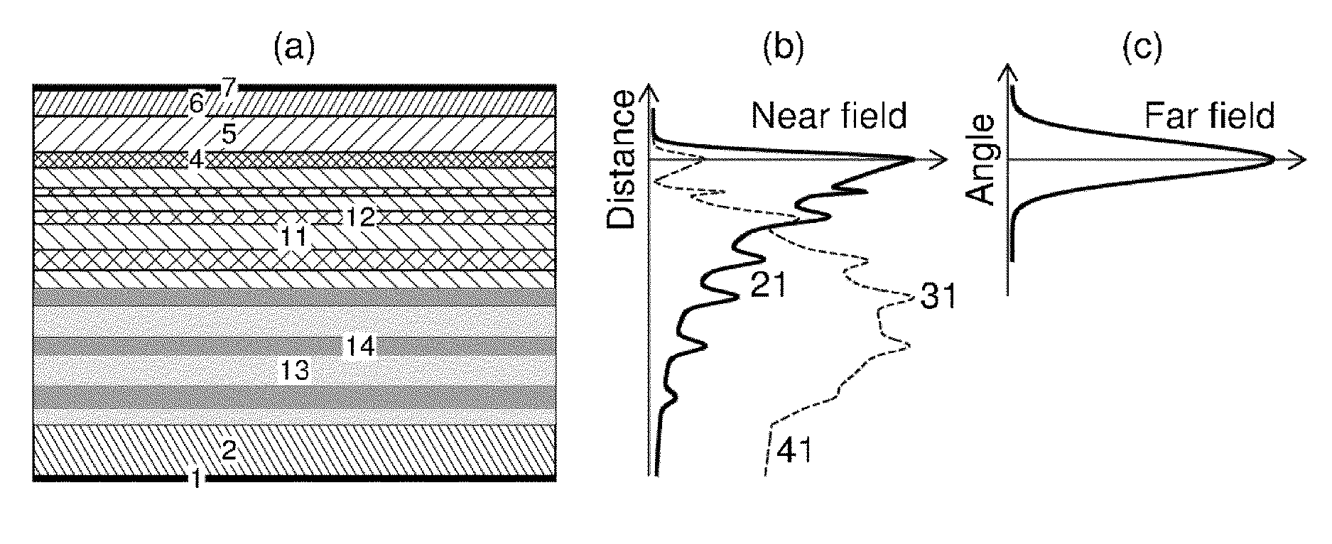
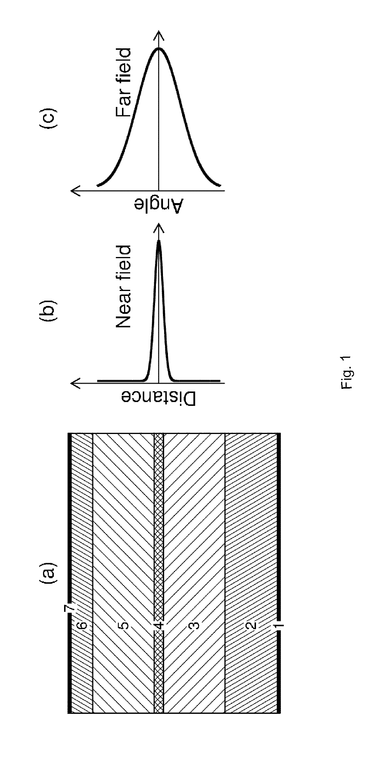
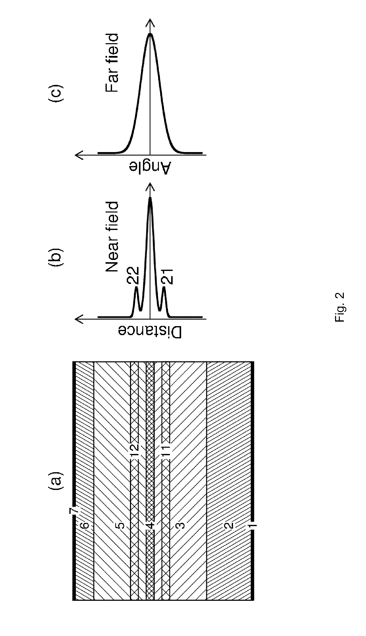
[0083]FIG. 13 shows an optical device 100 for generating short optical pulses Pcomp. The device 100 comprises a single section semiconductor laser 110, an electrical control unit 120, and a dispersive element 130.

[0084]The electrical control unit 120 is connected to the single section semiconductor laser 110 and injects a DC current I which causes the laser to operate in a nonlinear regime. In this nonlinear regime, the ...


PUM


Abstract

An embodiment of the invention relates to a method for generating short optical pulses comprising the steps of:operating a single section semiconductor laser in a nonlinear regime to emit chirped optical pulses at an output facet of the laser cavity, andcompressing the chirped optical pulses outside the laser cavity using a dispersive element in order to generate the short optical pulses.

Description

BACKGROUND OF THE INVENTION[0001]High power laser systems emitting short optical pulses are useful for many emerging applications in materials processing, biotechnology, instrumentation, metrology and medicine, representing one of the fastest growing laser markets nowadays. In particular, semiconductor laser based systems can benefit from the higher efficiency, compactness, wavelength tunability, lower cost, as well as the reduced complexity and footprint of laser diodes when compared to commercially available Ti:sapphire and fiber lasers.[0002]The generation of optical pulses in semiconductor laser diodes is commonly achieved by means of gain switching, by driving the laser diode with an electrical injection of high peak current pulses having a duration of a few hundred picoseconds. The minimum pulse width that can be achieved with this technique is typically of a few tens of picoseconds which is in many cases longer than required by most applications. Besides, the average power is...

Claims


Application Information

Patent Timeline
Patent Type & Authority Patents(United States)
IPC IPC(8): H01S3/00H01S5/062H01S5/065H01S3/067
CPCH01S3/0057H01S3/067H01S5/0657H01S5/06216H01S5/0287H01S5/0604H01S5/2036H01S5/3213H01S5/3216H01S2301/166H01S2301/18
Inventor ROSALES, RICARDOBIMBERG, DIETER
Owner TECH UNIV BERLIN
Why Eureka
Try Eureka