Power loss protection integrated circuit

a technology of power loss protection and integrated circuit, which is applied in the direction of emergency power supply arrangements, electric controllers, instruments, etc., can solve the problems of insufficient energy storage, achieve high voltage, reduce power signals, and signal fast

Active Publication Date: 2017-07-11
ACTIVE SEMI
View PDF3 Cites 20 Cited by
  • Summary
  • Abstract
  • Description
  • Claims
  • Application Information

AI Technical Summary

Benefits of technology

[0006]In a second novel aspect, a single power loss protection integrated circuit includes a current switch circuit (that can perform the eFuse function), an input voltage terminal (VIN), an output voltage terminal (VOUT), a buck / boost controller, and a storage capacitor terminal (STR). The buck / boost controller is adapted to work, along with discrete components external to the integrated circuit such as a discrete inductor, as either a buck converter in a buck mode of operation, or as a boost converter in a boost mode of operation. The same external inductor is used as the inductor in both modes. In the boost mode, the buck / boost controller drives a switch terminal so that the buck / boost controller in combination with the external inductor receives a relatively low voltage as output by the current switch circuit (the eFuse) and outputs a relatively high voltage onto the storage capacitor terminal (STR) thereby charging any external capacitor coupled to this terminal. In the buck mode, the buck / boost controller receives the relatively high voltage from the storage capacitor terminal (STR) and bucks it down to the relatively low voltage that is required at the output voltage terminal VOUT by the device to be powered. The current switch circuit in performing its eFuse function can pass a through-current of up to a maximum current from the input voltage terminal VIN to the output voltage terminal VOUT, where this maximum input current is a large current of at least two amperes. The through-current is large as compared to currents that typically pass through digital logic circuits. The current switch circuit outputs a digital undervoltage signal and a digital high current signal. The digital undervoltage signal (UV), if asserted, indicates that the input voltage on the VIN terminal is lower than a predetermined voltage. The digital high current signal (HC), if asserted, indicates that the through-current is greater than a predetermined current. If the digital undervoltage signal UV is asserted, then the buck / boost converter is made to begin operating in the buck mode. If the digital high current signal HC is asserted, then the buck / boost converter is prevented from operating in the boost mode. Advantageously, the intercommunication of the necessary signals between the current switch circuit portion of the integrated circuit and the buck / boost controller portion of the integrated circuit to accomplish these conditional disabling functions are on the integrated circuit. This allows the signaling to be fast, and allows the signals to be lower power signals because the environment on-chip is relatively free of potential noise problems that otherwise might be present were the intercommunication to have to pass across conductors on a printed circuit board. Potential board level complexities and noise problems are avoided. The speed and efficiency of the intercommunication allows the size of the storage capacitor bank for a given application to be made smaller and less expensive because the buck / boost converter is controlled faster in a fault condition as compared to a prior art situation as illustrated in FIG. 1 of the background information section.

Problems solved by technology

When the power loss protection system is needed in a power loss event, the remainder of the circuit works but there may be inadequate energy stored due to the lower than required capacitance where the backup energy is stored.

Method used


Image

  • Power loss protection integrated circuit
  • Power loss protection integrated circuit
  • Power loss protection integrated circuit

Examples


Embodiment Construction

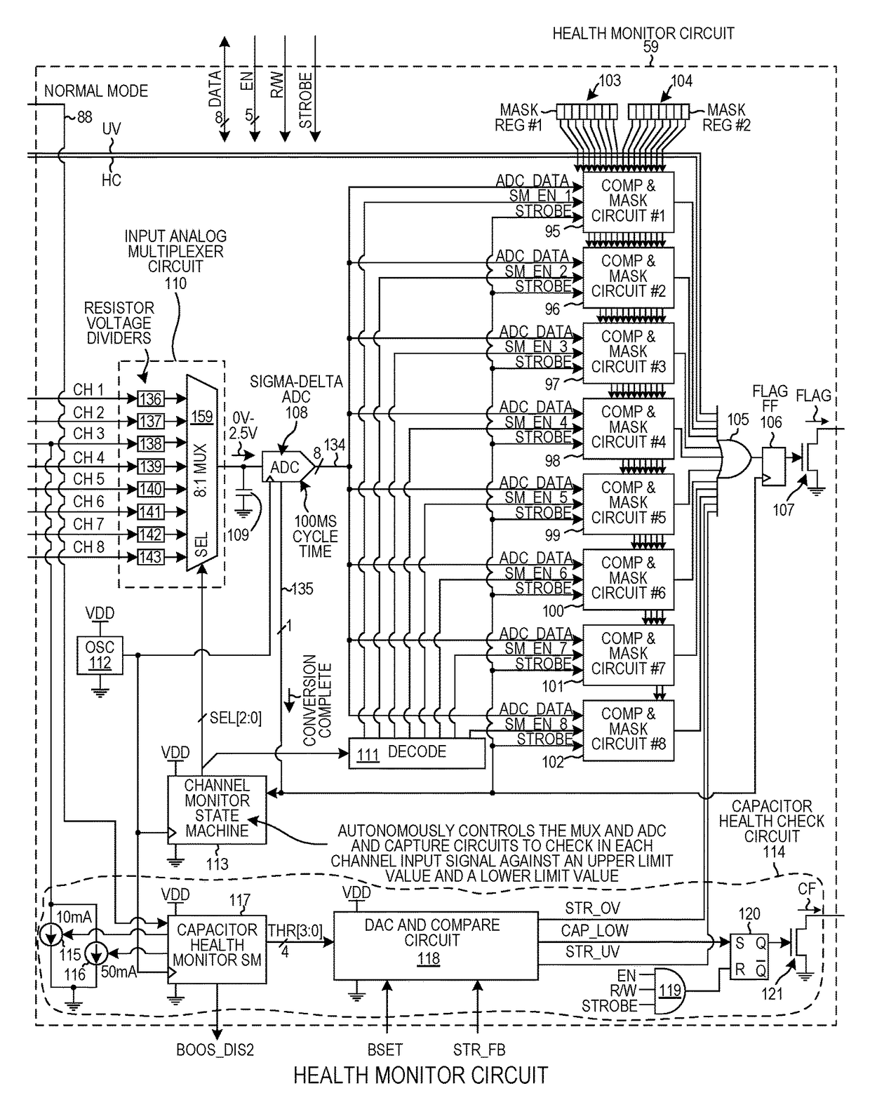
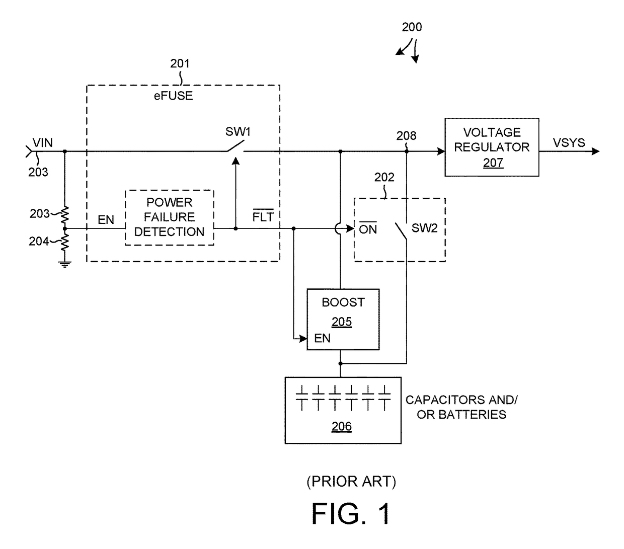
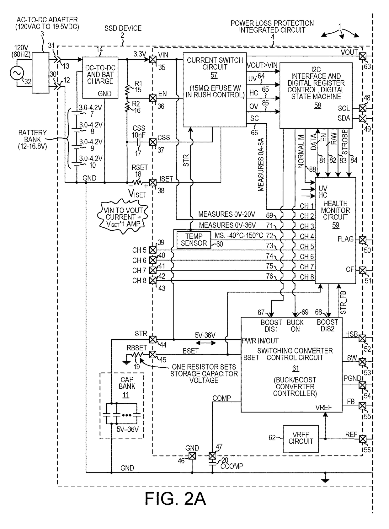
[0024]FIG. 2 is a diagram of a system 1 that involves a device to be powered 2 and an AC-to-DC adapter 3. The device 2 in this particular example is a Solid State Drive (SSD) device. It includes a solid state device system 4, a Power Management Unit (PMU) integrated circuit 5, a power loss protection integrated circuit 6, a bank of series-connected batteries 7-10, a bank of parallel-connected capacitors 11, a socket portion 12 and 13 of a connector, a DC-to-DC converter and battery charger 14, and other discrete components 15-29. The solid state drive system 4 includes, among other components not shown, a solid state memory portion 33 and a microcontroller integrated circuit 34. The AC-to-DC adapter 3 can be connected to the SSD device 2 by plugging its plug portion 30 and 31 into the socket portion 12 and 13 of the SSD device, and the AC-to-DC adapter 3 can be disconnected from the SSD device by unplugging it from the socket portion. The AC-to-DC adapter 3 is coupled to receive pow...


PUM


Abstract

A power loss protection integrated circuit includes a current switch circuit (eFuse), a VIN terminal, a VOUT terminal, a buck/boost controller, and a storage capacitor terminal STR. The controller is adapted to work: 1) as a boost to take a low voltage from the VOUT terminal and to output a larger charging voltage onto the STR terminal, or 2) as a buck to take a higher voltage from the STR terminal and to buck it down to a lower voltage required on the VOUT terminal. The current switch circuit outputs a digital undervoltage signal (UV) and a digital high current signal (HC). These signals are communicated on-chip to the controller. Asserting UV causes the converter to begin operating in the buck mode. Asserting HC prevents the converter from operating in the boost mode.

Description

CLAIM OF PRIORITY UNDER 35 U.S.C. §119[0001]This application claims the benefit under 35 U.S.C. §119 of each of the following six U.S. Provisional Applications: 1) U.S. Provisional Application Ser. No. 62 / 354,732, entitled “POWER INTEGRATED CIRCUIT WITH AUTONOMOUS LIMIT CHECKING OF ADC CHANNEL MEASUREMENTS,” filed Jun. 25, 2016; 2) U.S. Provisional Application Ser. No. 62 / 354,733, entitled “POWER LOSS PROTECTION INTEGRATED CIRCUIT,” filed Jun. 25, 2016; 3) U.S. Provisional Application Ser. No. 62 / 354,734, entitled “AUTONOMOUS CAPACITOR HEALTH CHECK IN A POWER LOSS PROTECTION INTEGRATED CIRCUIT,” filed Jun. 25, 2016; 4) U.S. Provisional Application Ser. No. 62 / 354,738, entitled “PROGRAMMABLE VOLTAGE SETTING WITH OPEN AND SHORT CIRCUIT PROTECTION,” filed Jun. 25, 2016; 5) U.S. Provisional Application Ser. No. 62 / 354,740, entitled “OPTIMIZED GATE DRIVER FOR LOW VOLTAGE POWER LOSS PROTECTION SYSTEM,” filed Jun. 25, 2016; 6) U.S. Provisional Application Ser. No. 62 / 354,741, entitled “FAS...

Claims


Application Information

Patent Timeline
Patent Type & Authority Patents(United States)
IPC IPC(8): H02M3/158H02M1/32H02M1/08H02M3/156H02M1/00
CPCH02M3/1582H02M1/08H02M3/1588H02M3/158H02M3/156H02M1/32H02M2001/0009H03M1/122H03M1/765H02J9/061G05F1/66G06F2201/81G06F11/0757G06F11/3013G06F11/3062G06F1/30H01H85/0241G01R31/3835G01R27/2605G01R31/392G01R31/64H02M1/0009G01R19/2513G05B11/28G05B15/02H02H3/08
Inventor CARPENTER, JR., JOHN H.SMITH, BRETT E.WATANABE, HIROSHI
Owner ACTIVE SEMI
Why Eureka
Try Eureka