Multi-level stacked transistor device including capacitor and different semiconductor materials

a transistor and multi-layer technology, applied in the field of semiconductor devices, can solve the problems of insufficient operation speed of a transistor including an oxide semiconductor, power consumption of the semiconductor device due to current, and the inability to ignore the current in the state, so as to achieve high integration and reduce power consumption.

Inactive Publication Date: 2017-09-05
SEMICON ENERGY LAB CO LTD
View PDF140 Cites 8 Cited by
  • Summary
  • Abstract
  • Description
  • Claims
  • Application Information

AI Technical Summary

Benefits of technology

[0007]High performance (for example, high-speed operation and low power consumption) of a semiconductor device such as an integrated circuit (IC) has been achieved through miniaturization and high integration of a semiconductor element formed using single crystal silicon or the like. However, power consumption of the semiconductor device due to current when a transistor is in an off state (referred to as off-state current or leakage current) increases as miniaturization and high integration of the semiconductor element progress; thus, the off-state current cannot now ignore.
[0009]Thus, an object of one embodiment of the disclosed invention is to provide a semiconductor device having a novel structure in which a transistor including an oxide semiconductor and a transistor including a semiconductor material which is not an oxide semiconductor are stacked. Another object is to provide a semiconductor device having a novel structure and lower power consumption.
[0010]Another object is to provide a semiconductor device in which a semiconductor element and a capacitor are formed efficiently.
[0026]A semiconductor device having a novel structure in which a transistor including an oxide semiconductor and a transistor including a semiconductor material which is not an oxide semiconductor are stacked can be provided. Further, in the semiconductor device having a novel structure, power consumption can be reduced. Furthermore, in the semiconductor device having a novel structure, a semiconductor element can be highly integrated.
[0027]In addition, a semiconductor device in which a semiconductor element and a capacitor are formed efficiently can be provided.

Problems solved by technology

However, power consumption of the semiconductor device due to current when a transistor is in an off state (referred to as off-state current or leakage current) increases as miniaturization and high integration of the semiconductor element progress; thus, the off-state current cannot now ignore.
On the other hand, the operation speed of a transistor including an oxide semiconductor is not sufficiently high compared with that of a transistor including a semiconductor material which is not an oxide semiconductor, such as single crystal silicon.

Method used


Image

  • Multi-level stacked transistor device including capacitor and different semiconductor materials
  • Multi-level stacked transistor device including capacitor and different semiconductor materials
  • Multi-level stacked transistor device including capacitor and different semiconductor materials

Examples


embodiment 1

[0052]In this embodiment, a semiconductor device of one embodiment of the present invention and a method for manufacturing the semiconductor device will be described with reference to FIG. 1, FIG. 2, FIG. 3, FIG. 4, FIG. 5, FIGS. 6A to 6D, FIGS. 7A to 7E, FIGS. 8A to 8D, and FIGS. 9A to 9C.

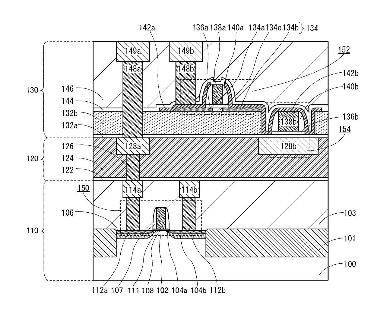
[0053]FIG. 1 is a cross-sectional view illustrating an example of a structure of a semiconductor device. A semiconductor device illustrated in FIG. 1 includes a transistor 150 which includes a semiconductor formed using a first semiconductor material, a wiring 128a formed over the transistor 150, a transistor 152 formed over the transistor 150, and a capacitor 154 formed over the transistor 150. FIG. 1 illustrates a structure in which a first semiconductor element layer 110 including the transistor 150 formed using the first semiconductor material is provided in a lower portion, and the transistor 152 formed using a second semiconductor material and a second semiconductor element layer 130 includi...

embodiment 2

[0226]In this embodiment, a semiconductor device which is different from the semiconductor device described in Embodiment 1 and a method for manufacturing the semiconductor device will be described with reference to FIG. 10, FIGS. 11A to 11D, and FIGS. 12A and 12B.

[0227]FIG. 10 is a cross-sectional view illustrating an example of a structure of a semiconductor device. A semiconductor device illustrated in FIG. 10 includes a transistor 150 in which includes a semiconductor formed using a first semiconductor material, a wiring 128a formed over the transistor 150, a transistor 166 formed over the transistor 150, and a capacitor 168 formed over the transistor 150. FIG. 10 illustrates a structure in which a first semiconductor element layer 110 including the transistor 150 formed using the first semiconductor material is provided in a lower portion, and part of the transistor 166 formed using a second semiconductor material and a second semiconductor element layer 170 including part of t...

embodiment 3

[0258]In this embodiment, the semiconductor device described in the above embodiment which can hold stored data even when power is not supplied and does not have a limitation on the number of write cycles will be described with reference to FIGS. 13A and 13B.

[0259]FIG. 13A illustrates an example of a circuit configuration of a semiconductor device, and FIG. 13B is a conceptual diagram illustrating an example of a semiconductor device. First, the semiconductor device illustrated in FIG. 13A will be described, and then, the semiconductor device illustrated in FIG. 13B will be described.

[0260]In the semiconductor device illustrated in FIG. 13A, a bit line BL is electrically connected to a source electrode or a drain electrode of a transistor 252, a word line WL is electrically connected to the gate electrode of the transistor 252, and the source electrode or the drain electrode of the transistor 252 is electrically connected to a first terminal of a capacitor 254. Here, the transistor ...


PUM


Abstract

A semiconductor device having a novel structure is provided in which a transistor including an oxide semiconductor and a transistor including a semiconductor material which is not an oxide semiconductor are stacked. Further, a semiconductor device in which a semiconductor element and a capacitor are formed efficiently is provided. In a semiconductor device, a first semiconductor element layer including a transistor formed using a semiconductor material which is not an oxide semiconductor, such as silicon, and a second semiconductor element layer including a transistor formed using an oxide semiconductor are stacked. A capacitor is formed using a wiring layer, or a conductive film or an insulating film which is in the same layer as a conductive film or an insulating film of the second semiconductor element layer.

Description

BACKGROUND OF THE INVENTION[0001]1. Field of the Invention[0002]The technical field of the present invention relates to a semiconductor device. Here, semiconductor devices refer to general elements and devices which function utilizing semiconductor characteristics.[0003]2. Description of the Related Art[0004]Attention has been focused on a technique for forming a transistor using a semiconductor thin film formed over a substrate having an insulating surface. The transistor is applied to a wide range of electronic devices such as an integrated circuit (IC). A silicon-based semiconductor material is widely known as a material for a semiconductor thin film applicable to a transistor. As another material, an oxide semiconductor has been attracting attention.[0005]For example, a transistor including a semiconductor thin film formed using an amorphous oxide containing indium (In), gallium (Ga), and zinc (Zn) (In—Ga—Zn—O-based amorphous oxide) is disclosed (see Patent Document 1).REFERENCE...

Claims


Application Information

Patent Timeline
Patent Type & Authority Patents(United States)
IPC IPC(8): H01L29/786H01L27/12
CPCH01L29/78693H01L27/1225H01L27/1255
Inventor ISOBE, ATSUOARAI, YASUYUKI
Owner SEMICON ENERGY LAB CO LTD
Why Eureka
Try Eureka