Dual discharge modes operation for remote plasma

a plasma and remote technology, applied in the field of semiconductor systems, processes, equipment, etc., can solve the problems of deformation of remaining materials, local plasma damage to the substrate, wet processes may have difficulty in penetrating some constrained, etc., to increase the distance electrons travel, improve the densities of radicals, and improve the effect of semiconductor processing

Active Publication Date: 2017-09-26
APPLIED MATERIALS INC
View PDF1639 Cites 107 Cited by
  • Summary
  • Abstract
  • Description
  • Claims
  • Application Information

AI Technical Summary

Benefits of technology

[0006]A hollow cathode discharge may be a plasma discharge that increases the electron impact ionization rate at the center of a hollow cathode, a so-called virtual anode, by pendulum electrons emitted from a cathode surface under a particular pressure-diameter of hollow cathode (pD) condition. Generating a hollow cathode discharge for semiconductor processing, and possibly alternating generation of the hollow cathode discharge with generation of a glow discharge in the same processing chamber, may provide advantages in semiconductor processing.
[0010]Embodiments of the present technology may provide improvements in semiconductor processing. A hollow cathode discharge may be more stable at higher operating pressures. Higher pressure processing may allow for increased densities of radicals, ions, and other species. Hollow cathode discharges may also increase the distance that electrons travel, and the increased travel distance may increase the probability that an electron would collide with a neutral atom to ionize the atom and generate another electron. The increased densities may result in faster etching of or depositing on a semiconductor substrate. Additionally, possibly as a result of increased densities or different chemistries, processing with a hollow cathode may allow for a more selective process than conventional processing.
[0011]The ionization processes in a hollow cathode may result in electrons remaining in a cavity space defined by an electrode and may result in less damage to the electrode, increasing process reliability and equipment uptime. The hollow cathode discharge may increase the amount of electron impact ionization (i.e., alpha process) and decrease the amount of ionization from secondary electrons (i.e., gamma process). The increase in the amount of electron impact ionization may also decrease damage of cathode and anode surfaces. Moreover, operating a plasma in two different discharge modes may permit increased precision, control, and / or flexibility in semiconductor processing. Embodiments of the present technology provide these and other advantages.

Problems solved by technology

However, wet processes may have difficulty penetrating some constrained trenches and also may sometimes deform the remaining material.
However, local plasmas may damage the substrate through the production of electric arcs as they discharge or if a high enough selectivity is not achievable.

Method used


Image

  • Dual discharge modes operation for remote plasma
  • Dual discharge modes operation for remote plasma
  • Dual discharge modes operation for remote plasma

Examples


example 1

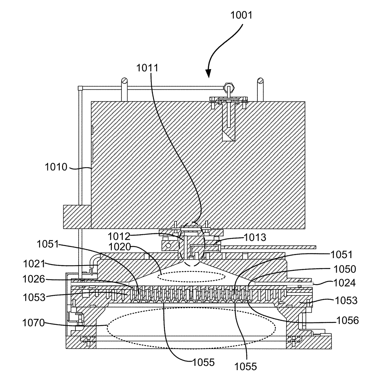
[0070]In this example, plasmas were generated in a system, where the total height of conical cavity defined by powered electrode is 10 cm. The diameter at the top of cavity was 0.5 cm, and the diameter at the bottom of cavity was 5 cm. Apertures in electrically grounded electrode have a diameter of 0.08 cm. Both the powered electrode and the electrically grounded electrode were made of nickel-coated aluminum without any dielectric coating. The setup was a direct-current type resistive plasma device, without a phase difference between voltage and current.

[0071]A commercial electronic ballast with a maximum power of 100 W was used to generate a plasma. The commercial electronic ballast in this example was an electronic ballast for household fluorescent lamps. The electronic ballast had an output frequency of 60 to 100 kHz and a 0 to 10 V control for dimming. The voltage was measured with a 100:1 voltage probe (PPE2 KV, LeCroy®), and the current was measured with a current probe (P6021...

example 2

[0073]From the system setup in Example 1, the peak voltages were 707 V and −290 V, as shown in FIG. 9(a). The positive and negative peak currents were 270 mA and −398 mA, respectively, as shown in FIG. 9(b). The voltage waveform was biased around 200 V. Pressure was varied between 1.5 Torr and 27 Torr. The voltage bias decreased with increasing pressure. In the positive half cycle, as the pressure increased, the voltage decreased and the current increased.

[0074]At 1.5 Torr, in the positive half cycle of the period with the powered electrode being an anode, the peak current was about 30 percent lower than that in the negative half cycle when the powered electrode was a cathode, even though the actual applied voltage was about 2.4 times higher. The total charge transferred during positive and negative cycles were 1.69 C and 1.65 C, respectively, which was only different by about 2.5%. The results imply that the discharge phenomena of the positive and negative half cycles may be differ...

example 3

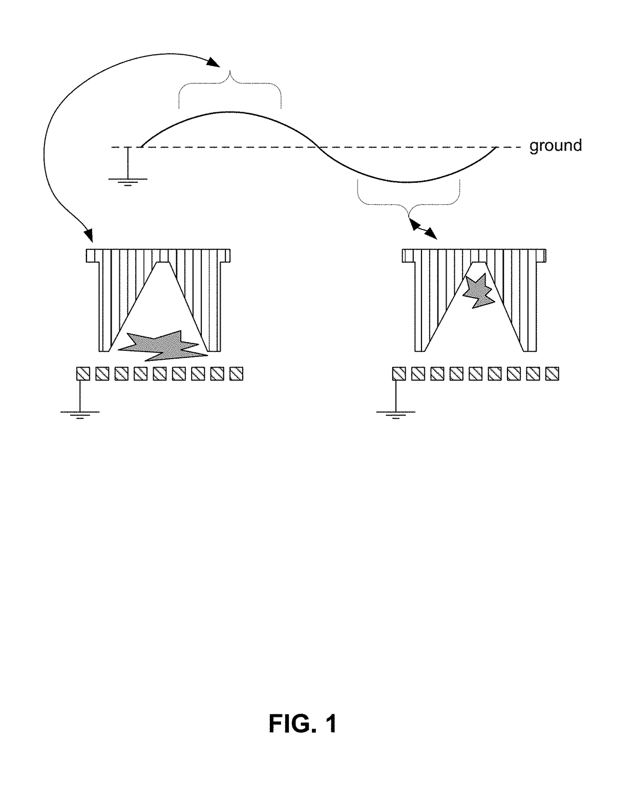
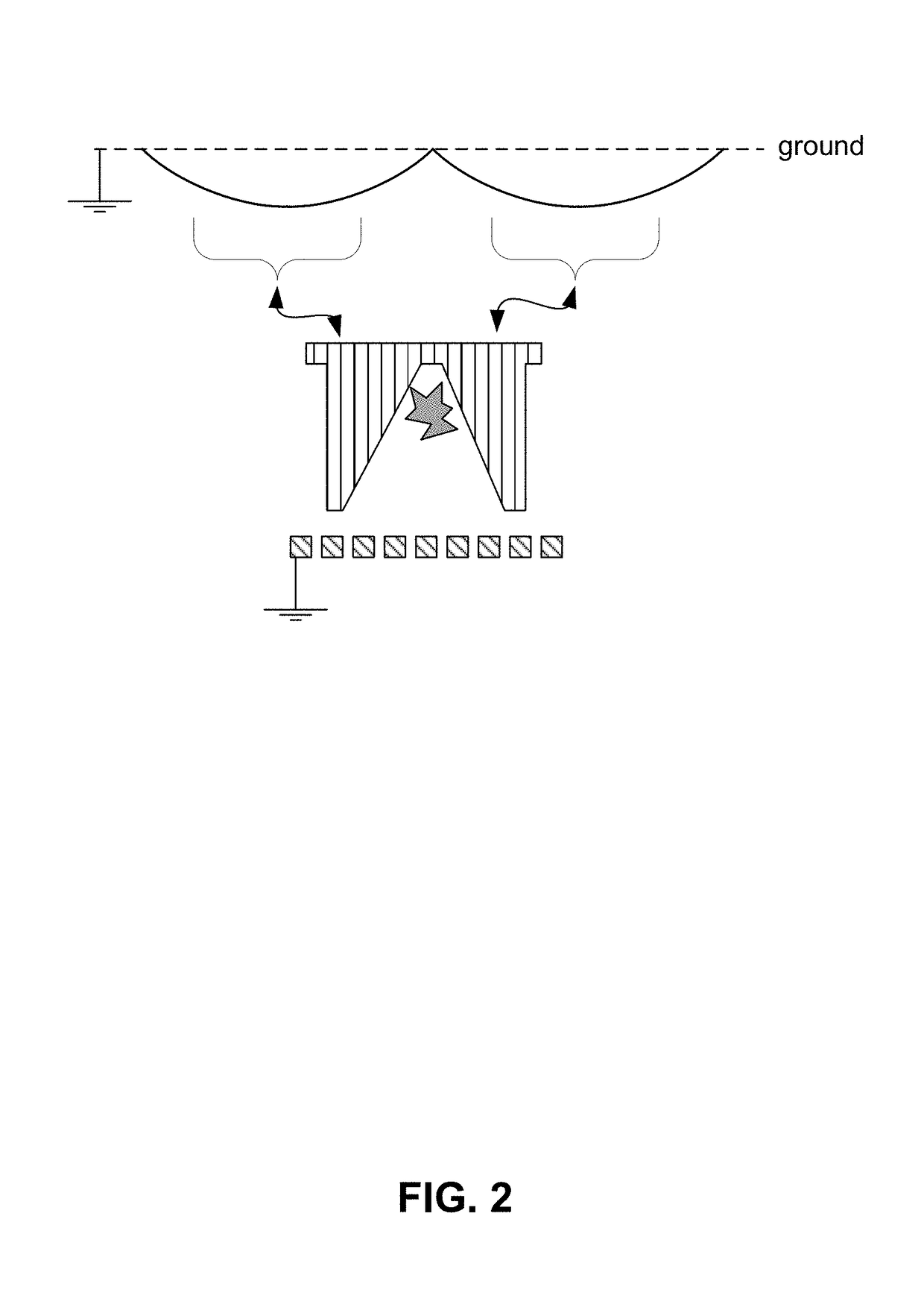
[0076]Time-resolved images from discharges generated in the system in Example 2 are shown in FIG. 10. The exposure time for these images was 0.5 μs. The images from the glow discharge appear different than the images from the hollow cathode discharge. The hollow cathode discharge images were observed to be more intense than the glow discharge images.

[0077]At 8.8 Torr, the glow discharge images show strong emissions in the ten o'clock direction of the grounded electrode. This observation, along with the electrical characteristics at this pressure in Example 2, suggests that a hollow cathode discharge may be present at a pressure of 8.8 Torr with a pD of about 0.7 Torr-cm (D=0.08 cm). As can be seen in the image, this discharge is not uniform, and may not be desirable for semiconductor processing.

[0078]The hollow cathode discharge mode in the negative half cycle was sustained up to 8.8 Torr and became more intense with increasing pressure. Because the diameter of the intense light emi...


PUM

PropertyMeasurementUnit
frequencyaaaaaaaaaa
pressureaaaaaaaaaa
pressureaaaaaaaaaa

Abstract

Embodiments of the present technology may include a method of processing a semiconductor substrate. The method may include providing the semiconductor substrate in a processing region. Additionally, the method may include flowing gas through a cavity defined by a powered electrode. The method may further include applying a negative voltage to the powered electrode. Also, the method may include striking a hollow cathode discharge in the cavity to form hollow cathode discharge effluents from the gas. The hollow cathode discharge effluents may then be flowed to the processing region through a plurality of apertures defined by electrically grounded electrode. The method may then include reacting the hollow cathode discharge effluents with the semiconductor substrate in the processing region.

Description

CROSS-REFERENCES TO RELATED APPLICATIONS[0001]This application claims the benefit of and priority to U.S. Provisional Application No. 61 / 872,064 filed Aug. 30, 2013 and titled “DUAL DISCHARGE MODES OPERATION FOR REMOTE PLASMA REMOVAL PROCESS OF SICONI / CHISEL”, the entire contents of which are hereby incorporated herein by reference for all purposes.FIELD[0002]The present technology relates to semiconductor systems, processes, and equipment. More specifically, the present technology relates to systems and methods for reducing film contamination and improving device performance.BACKGROUND[0003]Integrated circuits are made possible by processes which produce intricately patterned material layers on substrate surfaces. Producing patterned material on a substrate requires controlled methods for removal of exposed material. Chemical etching is used for a variety of purposes including transferring a pattern in photoresist into underlying layers, thinning layers, or thinning lateral dimensi...

Claims


Application Information

Patent Timeline
Patent Type & Authority Patents(United States)
IPC IPC(8): C23C14/32H01J37/32
CPCH01J37/32596H01J37/32018H01J37/32357H01J37/32449H01J37/32541H01J37/32568
Inventor CHO, TAE SEUNGSEN, YI-HENGPARK, SOONAMLUBOMIRSKY, DMITRY
Owner APPLIED MATERIALS INC
Why Eureka
Try Eureka